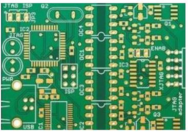
This article discusses the key steps of building a low electromagnetic interference (EMI) prototype before the microwave anechoic chamber conformance test, including designing low-radiation circuits and pre-compatibility testing. Pre-compatibility testing includes the use of 3D electromagnetic field simulation software to simulate the PCB layout model and EMI analysis, and then use the spectrum analyzer (SA) to perform near-field electromagnetic scanning of the prototype PCB. Finally, perform a microwave anechoic chamber test to verify the design.
Lowest EMI circuit design
To ensure low radiated emission (RE), best practice experience must be applied when designing circuit schematics and PCB layouts, including adding ferrite beads for power supply circuits, USB data lines, Ethernet and other signals to filter EMI. In addition, proper placement of a sufficient number of decoupling capacitors on the power supply loop can minimize the impedance of the power distribution network, thereby reducing the amplitude of the noise ripple generated by the digital load and reducing the risk of radiation. At the same time, the closed loop compensation network design of the switching power supply is optimized to achieve a stable closed loop, which can ensure that the voltage output is controllable and minimize the switching noise ripple amplitude. The reduced noise ripple amplitude can significantly suppress the EMI risk of the prototype.
PCB traces for high frequency or fast rising/falling edge signals should refer to the continuous loop (for example, refer to the ground plane) to reduce the risk of EMI. The trace cannot pass through any dividing planes and holes. If the signal needs to be transmitted between layers through vias, at least one ground via should be placed next to the signal via as a return path for signal current from the receiving end to the transmitting end. If there is no proper return path, the return current may be arbitrarily transmitted in the PCB and become a potential EMI source.

Excellent grounding scheme is also a key factor in minimizing EMI. All PCB designs must avoid ground loops, because the ground loops will form a radiating transmitter when the return signal current passes. Designing the ground as a wide reference plane can construct an excellent grounding scheme. The ground planes of different circuit groups (such as radio frequency, analog and digital circuits) should be physically separated, and circuit connections should be established through ferrite beads to help prevent high-frequency noise from spreading between circuit groups.
After completing the PCB layout design, simulation should be performed for EMI analysis to ensure that the PCB has a low risk of radiation emission before manufacturing. Omitting EMI simulation may not guarantee the EMI performance of the PCB, and will lead to redesign. If the EMI simulation results meet the technical specifications, the designer can start PCB manufacturing, and then use a spectrum analyzer to perform near-field electromagnetic scanning on the prototype PCB. Pre-compatibility testing such as EMI simulation and near-field electromagnetic scanning can increase the designer's confidence that the prototype has lower EMI. After the pre-compatibility test is completed, the device under test can perform the actual EMI compliance test in the anechoic chamber.
Simulation EMI analysis
After completing the PCB layout design, import the layout file into EMPro 2013.07 to perform 3D EMI simulation. The differential signal is selected for finite element method (FEM) three-dimensional electromagnetic field simulation. Three-dimensional electromagnetic field simulation is the process of setting electromagnetic boundary conditions and model mesh size and solving Maxwell's equations. To ensure the accuracy of the simulation results, the boundary size should be set to more than 8 times the PCB thickness, and the grid size should be set to less than 1/5 of the PCB width. The computer running the three-dimensional electromagnetic field needs to be equipped with a memory of more than 16G and a storage capacity of more than 100G to ensure the smooth progress of the analysis.
Set up a far-field sensor to capture the emitted electromagnetic field, and use EMPro's EMI simulation template to calculate the far-field emission power, and then set up an electric field probe at a distance of 10m to draw a frequency domain response graph. Then perform the three-dimensional electromagnetic field simulation of the finite difference time domain method (FDTD) mode, and compare with the simulation results of the FEM mode.
Refer to the simulation diagram of electric field intensity at 30MHz~1GHz (Figure 1) (the unit of electric field intensity is dBμV, the frequency unit is GHz), the radiation power level (blue curve is FEM mode simulation, red curve is FDTD mode simulation) is lower than about 45dBμV FCC maximum threshold (green dashed line).
A peak of maximum power intensity (-66.4dBm) appears near 400MHz. The coil as the near-field sensor moves within 3 inches from the device under test. The 30kHz spectrum analyzer resolution bandwidth can achieve low noise floor (-80dBm) measurement, so the spikes (radiation of different discrete frequencies) are clearly visible. To enhance the confidence that the prototype passes the far-field (3m and 10m) EMI compliance test of the microwave anechoic chamber, the peak power in the near area should be lower than -65dBm. The red line shows the maximum radiated emission power level of CISPR 11 Class A: less than 56dBμV in the frequency range of 30MHz to 1GHz. The brown curve below the red line represents the guard band specified in the EMC guidelines of Keysight (formerly Agilent). The vertical and horizontal components of the radiation wave are represented by blue and green curves, respectively. Two power peaks of 38dBμV and 37dBμV appear at 400MHz and 560MHz frequencies, and both are below the maximum threshold.
Low-EMI circuit design and pre-compatibility testing (such as three-dimensional EMI simulation and near-field electromagnetic scanning) are very important. They can avoid unnecessary PCB remanufacturing, save development costs and time, and can shorten the time of EMI compliance testing in microwave anechoic chambers to ensure electronics The device is put on the market on time or even in advance.
A. Electrolytic Ni/Au: This kind of coating is the most stable, but the price is the highest.
b. Immersion silver board (Immersiog AG) is not as good as gold-plated coating, and it is prone to electromigration and leakage.
c. Electroless nickel/gold plate (ElectrolessNickel? ImmersionAu, ENIG), when the immersion gold process is unstable, it is easy to produce black disk.
d. Electroless Tin, the lead-free immersion tin is not yet fully mature.
e. Hot air screed (Sn/Ag/CuHASL), the production process of this coating is not yet fully mature.
f. Organic Solderability Preservations (OSP, OrganicSolderabilityPreservations), this kind of coating is the cheapest, but the performance is the worst. When using an OSP board, pay attention to the storage time of the board between reflow and between reflow and wave soldering, because the protective film on the board pad is damaged after high temperature heating, and the solderability will be greatly reduced.