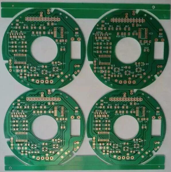
The process of printed circuit board from light board to display circuit pattern is a relatively complicated process of physical and chemical reaction. At present, the typical process of printed circuit board(PCB) processing adopts the "pattern plating method".

is to pre-plat a lead-tin anti-corrosion layer on the part of the copper foil that needs to be retained on the outer layer of the board, that is, the pattern part of the circuit, and then chemically corrode the remaining copper foil, which is called etching.
The etching method is a method of removing the copper foil other than the conductive circuit with an etching solution. The engraving method is a method of removing the copper foil other than the conductive circuit with an engraving machine. The former is a chemical method, which is more common, and the latter is a physical method.
PCB board etching introduction
The process of printed circuit board from light board to display circuit patternis a relatively complicated process of physical and chemical reaction. At present, the typical process of printed circuit board (PCB) processing adopts the "pattern plating method".
is to pre-plat a lead-tin anti-corrosion layer on the part of the copper foil that needs to be retained on the outer layer of the board, that is, the pattern part of the circuit, and then chemically corrode the remaining copper foil, which is called etching.
The etching method is a method of removing the copper foil other than the conductive circuit with an etching solution. The engraving method is a method of removing the copper foil other than the conductive circuit with an engraving machine. The former is a chemical method, which is more common, and the latter is a physical method.
PCB board etching problem
Reduce undercut and edge, improve etching coefficient
Lateral erosion produces a sharp edge. Generally, the longer the printed board is in the etching solution, the more serious the side etching. Undercutting seriously affects the accuracy of printed wires, and severe undercutting will make it impossible to make fine wires. When the undercut and the edge are reduced, the etching coefficient increases. A high etching coefficient indicates the ability to maintain thin wires and make the etched wires close to the size of the original image.
Whether it is tin-lead alloy, tin, tin-nickel alloy or nickel, if the electroplating etching resist is too high, it will cause the wire to short circuit. Because the protruding edge is easily broken, an electrical bridge is formed between the two points of the wire.
Universal PCB board introduction
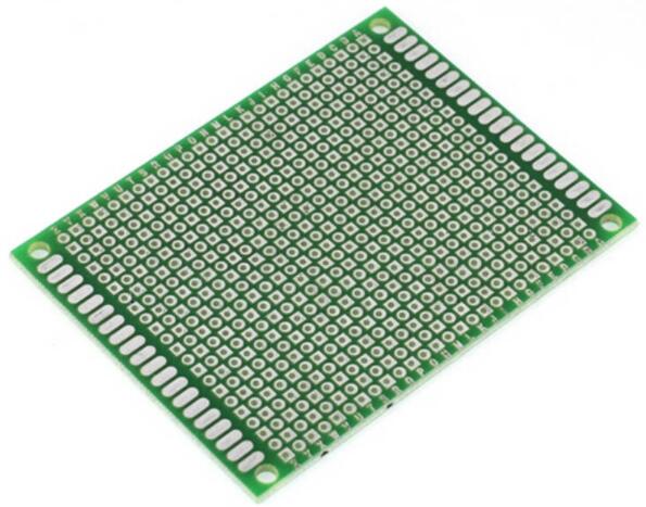
Universal PCB board is a kind of printed circuit board which is filled with pads according to the standard IC pitch (2.54mm), and can be inserted and connected according to your own wishes. It is commonly known as "hole board". Compared with professional PCB plate making, the hole-hole board has the following advantages: low threshold for use, low cost, convenient use, and flexible expansion. For example, in electronic design competitions for college students, works usually need to be completed within a few days of race against time, so holes are mostly used.

Universal PCB board introduction
Universal PCB board is when designing and developing electronic products, because some experiments need to be done, it is too slow for manufacturers to make PCB board and it is inconvenient to make frequent changes in the experimental stage, so the universal board was born.
Precautions for welding universal board
1. The layout of components must be reasonable, and it must be planned in advance. It is better to draw on paper first to simulate the process of routing. For signals with larger currents, the influence of contact resistance, ground loop, wire capacity, etc. should be considered. Single-point grounding can solve the influence of ground loops, which is easy to be overlooked.
Second, use wires of different colors to represent different signals (the same signal is best to use one color);
3. According to the circuit principle, make and debug step by step. You can test and debug a part of it. Don't wait until all the circuits are completed before testing and debugging, otherwise it is not conducive to debugging and troubleshooting.
Fourth, the wiring should be regular; make a mark on the schematic diagram while soldering.
5. Pay attention to the welding process. Especially the tin plating of the pins to be soldered.
1. If the pad of the universal board has been oxidized, then it needs to be polished with water gauze until the sand is bright. After drying, apply alcohol rosin solution and dry it for later use.
2. If the component pins are oxidized, scrape off the oxide layer with a blade or other tools, and then do tin plating for soldering;
3. After the wire is stripped, the insulation stripping length should be controlled to avoid short circuit with other wires after soldering;
4. Both ends of the wire need to be tinned before being soldered.
5. The welding process is in accordance with the five-step welding requirements.
etching problem
Reduce undercut and edge, improve etching coefficient
Lateral erosion produces a sharp edge. Generally, the longer the printed board is in the etching solution, the more serious the side etching. Undercutting seriously affects the accuracy of printed wires, and severe undercutting will make it impossible to make fine wires. When the undercut and the edge are reduced, the etching coefficient increases. A high etching coefficient indicates the ability to maintain thin wires and make the etched wires close to the size of the original image.
Whether it is tin-lead alloy, tin, tin-nickel alloy or nickel, if the electroplating etching resist is too high, it will cause the wire to short circuit. Because the protruding edge is easily broken, an electrical bridge is formed between the two points of the wire.
Universal PCB board introduction
Universal PCB board is a kind of printed circuit board which is filled with pads according to the standard IC pitch (2.54mm), and can be inserted and connected according to your own wishes. It is commonly known as "hole board". Compared with professional PCB plate making, the hole-hole board has the following advantages: low threshold for use, low cost, convenient use, and flexible expansion. For example, in electronic design competitions for college students, works usually need to be completed within a few days of race against time, so holes are mostly used.
Universal PCB board introduction
Universal PCB board is when designing and developing electronic products, because some experiments need to be done, it is too slow for manufacturers to make PCB board and it is inconvenient to make frequent changes in the experimental stage, so the universal board was born.
Precautions for welding universal board
1. The layout of components must be reasonable, and it must be planned in advance. It is better to draw on paper first to simulate the process of routing. For signals with larger currents, the influence of contact resistance, ground loop, wire capacity, etc. should be considered. Single-point grounding can solve the influence of ground loops, which is easy to be overlooked.
Second, use wires of different colors to represent different signals (the same signal is best to use one color);
3. According to the circuit principle, make and debug step by step. You can test and debug a part of it. Don't wait until all the circuits are completed before testing and debugging, otherwise it is not conducive to debugging and troubleshooting.
Fourth, the wiring should be regular; make a mark on the schematic diagram while soldering.
5. Pay attention to the welding process. Especially the tin plating of the pins to be soldered.
1. If the pad of the universal board has been oxidized, then it needs to be polished with water gauze until the sand is bright. After drying, apply alcohol rosin solution and dry it for later use.
2. If the component pins are oxidized, scrape off the oxide layer with a blade or other tools, and then do tin plating for soldering;
3. After the wire is stripped, the insulation stripping length should be controlled to avoid short circuit with other wires after soldering;
4. Both ends of the wire need to be tinned before being soldered.
5. The welding process is in accordance with the five-step welding requirements.