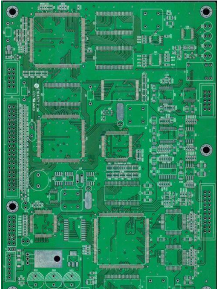
1. If the circuit system of the PCB design contains FPGA devices, the Quartus II software must be used to verify the pin assignments before drawing the schematic. (Some special pins in FPGA cannot be used as ordinary IO).
2, 4-layer board from top to bottom: signal plane layer, ground, power, signal plane layer; 6-layer board from top to bottom: signal plane
Layer, ground, signal inner electric layer, signal inner electric layer, power supply, signal plane layer. For boards with 6 layers or more (the advantage is: anti-interference radiation), the internal electrical layer wiring is preferred, and the plane layer cannot be walked away. It is forbidden to wire from the ground or power layer (reason: the power layer will be divided, causing parasitic effects).
3. Wiring of multi-power supply system: If FPGA+DSP system is made of 6-layer board, there will be at least 3.3V+1.2V+1.8V+5V. 3.3V is generally the main power supply, and the power layer is directly laid, and it is easy to route the global power network through vias; 5V may generally be the power input, and only a small area of copper is required. And as thick as possible.
1.2V and 1.8V are the core power supply (if you directly use the wire connection method, you will encounter great difficulties when facing BGA devices). Try to separate 1.2V and 1.8V during layout, and let 1.2V or 1.8V connect The components are arranged in a compact area and connected by copper

In short, because the power supply network is all over the entire PCB, if the PCB routing method is used, it will be very complicated and will go around a long distance. The method of using copper skin is a good choice!
4. The wiring between adjacent layers adopts a cross method: it can reduce electromagnetic interference between parallel wires and facilitate wiring.
5. What is the isolation method for analog and digital isolation? Separate the devices used for analog signals from those used for digital signals during layout, and then
One size fits all AD chips!
The analog signal is laid with an analog ground, and the analog ground/analog power supply and the digital power supply are connected at a single point through an inductor/magnetic bead.
6. PCB design based on PCB design software can also be regarded as a software development process. Software engineering pays most attention to the idea of "iterative development" to reduce the probability of PCB errors.
(1) Check the schematic diagram, pay special attention to the power and ground of the device (power and ground are the blood of the system, and there can be no negligence);
(2) PCB package drawing (confirm whether the pins in the schematic diagram are wrong);
(3) After confirming the PCB package size one by one, add a verification label and add it to the package library of this design;
(4) Import the netlist, adjust the signal sequence in the schematic while layout (OrCAD component automatic numbering function can no longer be used after layout);
(5) Manual wiring (check the power ground network while cloth, as I said before: the power network uses the copper method, so use less wiring);
In short, the guiding ideology in PCB design is to feed back and correct the schematic diagram while drawing the package layout (considering the correctness of signal connection and the convenience of signal routing).
7. The crystal oscillator is as close as possible to the chip, and there is no wiring under the crystal oscillator, and the network copper skin is laid. Clocks used in many places are wired in a tree-shaped clock tree.
8. The arrangement of the signals on the connector has a great influence on the difficulty of wiring, so it is necessary to adjust the signals on the schematic while wiring (but never renumber the components)
9. Design of multi-board connector:
(1) Use flat cable connection: the upper and lower interfaces are the same;
(2) Straight socket: the upper and lower interfaces are mirrored and symmetrical
10. Design of module connection signal:
(1) If two modules are placed on the same side of the PCB, then the control serial number will be connected to the smaller one (mirror connection signal);
(2) If two modules are placed on different sides of the PCB, the serial number of the control system should be connected to the smaller one and the larger one.