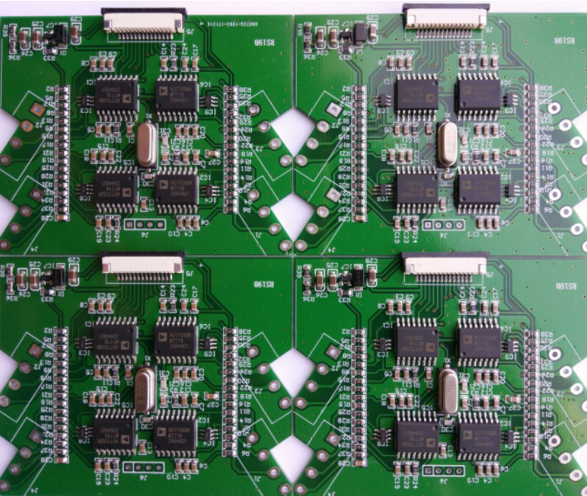
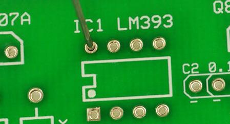
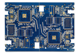
For PCB designers, the inductance of PCB vias is more important than capacitance. Each through hole has a parasitic inductance in the link. Because the physical structure of the through hole is small, its characteristics are very pixel lumped circuit elements. The main effect of the through-hole series inductance is to reduce the effectiveness of the power supply bypass capacitor, which will make the filtering effect of the entire power supply worse.
The purpose of the bypass capacitor is to short-circuit the two power planes together in the high frequency range. If it is assumed that an integrated circuit is connected between the power supply and the ground plane at point a, there is an ideal surface mount bypass capacitor at point b. It is expected that the high-frequency impedance between the vcs of the chip bonding point and the ground plane is zero. However, this is not the case. Each connection via inductance that connects the capacitor to the vcc and ground plane introduces a small but measurable inductance. The approximate size of this inductance is:
Among them, l=through hole inductance, nh
H=length of through hole, in
D=through hole diameter, in
Because the above formula includes a logarithm, the change in the diameter of the through hole has little effect on the inductance, but the change in the length of the through hole may cause a large change.
The inductance of the through hole to a signal with a rising edge speed of 1ns. First calculate the inductance:

H=0.063 (length of through hole, in)
D=0.016 (through hole diameter, in)
T10~90%=1.00 (rising edge speed, ns)
The high-frequency current is shunted from the chip, and the value of 3.8 ohms is not low enough. At the same time, keep in mind that one end of the bypass capacitor is usually connected to the ground plane through a through hole, and the other end is also connected to the +5v plane through a through hole, so the effect of through-hole inductance will be doubled. The bypass capacitor is mounted on the side of the board closest to the power and ground plane, which helps reduce its impact. Finally, any leads between the capacitor and the via will add more inductance. These traces should always be as wide as possible.
Using multiple bypass capacitors between the power supply and ground can get very low impedance. For digital products, as a rough guideline, assume that the power and ground planes are ideal conductors and the inductance is zero. We only consider the inductance of the bypass capacitor and its associated traces and vias. Within a certain range, all the bypass capacitors will be connected in parallel, reducing the impedance between the power supply and the ground. The effective radius that produces this effect is equal to 1/12, where 1 is the electrical length of the rising edge. Within 1/6 of the diameter, all capacitors collectively act as a lumped circuit.
The propagation length of the rising edge of 1ns in fr-4 material is about 1=6in. In this example, if the grid spacing of the capacitor is greater than 1/12=0.5in, there will be no benefit.
For the bypass capacitor of the power supply, the shorter the rise time, the more difficult the bypass will become. When the rise time is shortened, the value of the effective radius also becomes smaller. The number of capacitors in the effective radius decreases with the square of the rise time.
This is a comprehensive question. As the rise time decreases, the digital corner frequency increases, which increases the inductance of each via. The final result is that for a bypass capacitor with a specific configuration that works at a certain frequency, when the PCB factory halves the rise time, its effect will be reduced by 8 times. According to the ratio criterion, the experience gained from a working frequency range can be easily converted to a new working frequency range