1. The selected FR-4 is not the name of the material.
"FR-4" is often referred to as the code name. Flame retardant material. This means that the resin material must self-extinguish after burning. It is not a material name, but a material. Material grade, so there are many kinds of FR-4 grade materials used in general PCB circuit boards, but most of them are made of so-called Tera-Functionepoxy resin with filler and glass fiber. Made of this composite material. For example, it now has FR-4 water green fiberglass board and black fiberglass board, which has the functions of high temperature resistance, insulation, flame retardancy and so on. Therefore, when selecting materials, everyone must figure out the characteristics they need to achieve. You can easily buy the products you need.
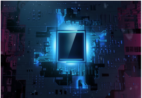
Flexible printed circuit boards (FPC) are also called flexible printed circuit boards or flexible printed circuit boards. Flexible printed circuit boards are products designed and manufactured on flexible substrates through printed circuits.
There are two main types of printed circuit board substrates: organic substrate materials and inorganic substrate materials, most of which are organic matrix materials. The PCB substrates used in different layers are also different. For example, 3-4 layers require prefabricated composite materials, and double-layer boards use glass epoxy materials.
2. When choosing a motherboard, we need to consider the impact of SMT

In the lead-free electronic assembly process, the bending degree of the printed circuit board when heated due to the increase in temperature increases, so it is necessary to use a small board curvature in the SMT, such as an FR-4 type substrate. Due to the influence of expansion and contraction stress on the components after the substrate is heated, the electrodes will be peeled off and reliability will be reduced. Therefore, special attention should be paid to the material expansion coefficient when selecting materials, especially when the component is larger than 3.2*1.6 mm. The PCB used in surface mount technology requires high thermal conductivity, excellent heat resistance (150°C, 60 minutes) and solderability (260°C, 10 s), and high copper foil adhesion strength (1.5*104 Pa) Or higher) and bending strength (25*104Pa), high conductivity, low dielectric constant, good punching performance (precision ±0.02mm), compatible with cleaning agents. In addition, the appearance is required to be smooth and flat, and warping, cracks, scratches and rust spots are not allowed.
3. PCB thickness selection
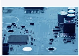
The thickness of the printed circuit board is 0.5mm, 0.7mm, 0.8mm, 1mm, 1.5mm, 1.6mm, (1.8mm), 2.7mm, (3.0mm), 3.2mm, 4.0mm, 6.4mm, of which 0.7mm and 1.5mm Thickness PCB is designed for gold finger dual-panel design, 1.8mm and 3.0mm non-standard sizes. From the perspective of production, the size of the printed circuit board should not be smaller than 250*200mm, and the ideal size is generally (250~350mm)*(200*250mm). The long side of the PCB is less than 125mm or the wide side is less than 100mm. Convenient to use the puzzle method. Surface assembly technology stipulates that the bending amount of a substrate with a thickness of 1.6mm is upper warpage ≤0.5mm and lower warpage ≤1.2mm. Generally, the allowable bending rate is less than 0.065%, which is divided into three types according to the metal material, as shown in a typical PCB. According to this structure, it is divided into three types, and electronic plug-ins have also been developed into large numbers, miniaturization, SMD and complexity. . The electronic plug-in is mounted on the circuit board by pins and soldered to the other side. This technology is called THT (Through Hole Technology) plug-in technology. In this way, each pin is drilled on the PCB, indicating the typical application of the PCB.
4. Drilling
With the rapid development of SMT chip technology, the multi-layers need to be drilled and electroplated to ensure the circuit board after transmission, which requires a variety of drilling equipment. In order to meet the above requirements, PCB CNC drilling equipment with different performance has been introduced at home and abroad. The production process of printed circuit boards is a complicated process. It involves a wide range of processes, mainly in the fields of photochemistry, electrochemistry and thermochemistry. In the manufacturing process, the number of process steps involved is also relatively large. Take a layer circuit board as an example to illustrate the processing steps. Drilling is an important process in the whole process. The hole processing time is also the longest. The position accuracy of the hole and the quality of the hole wall directly affect the metallization and repair of the subsequent hole, and also directly affect the printed circuit. The principle, structure and function of CNC drilling machine for plate processing quality and processing cost. Commonly used methods for drilling holes on circuit boards include CNC mechanical drilling methods and laser drilling methods. At this stage, the most commonly used method is mechanical drilling.