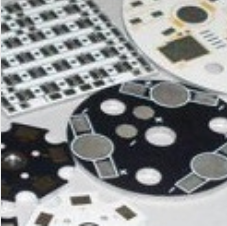
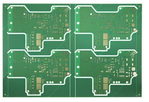
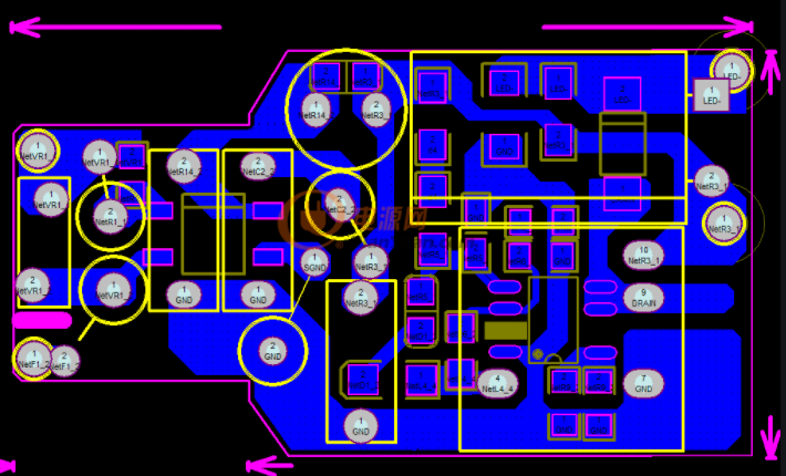
1. How to deal with some theoretical conflicts in actual PCB wiring--Q: In actual PCB wiring, many theories conflict with each other; for example: 1. Deal with the connection of multiple analog/digital grounds: theoretically it should be They are isolated from each other, but in actual miniaturization and high-density wiring, due to space limitations or absolute isolation, small-signal analog ground traces will be too long, making it difficult to achieve theoretical connections. The practice of the PCB factory is to divide the ground of the analog/digital functional module into a complete island, and the analog/digital ground of the functional module is connected to this island. Then connect the island to the "big" ground through the trench. I don’t know if this approach is correct? 2. In theory, the connection between the crystal oscillator and the CPU should be as short as possible. Due to the structural layout, the connection between the crystal oscillator and the CPU is relatively long and thin, so it is disturbed and the work is unstable. How to solve this problem from wiring? There are many other problems, especially EMC and EMI problems in high-speed PCB wiring. There are many conflicts, which is a headache. How to solve these conflicts?
Answer: 1. Basically, it is correct to separate the analog/digital ground. It should be noted that the signal trace should not cross the divided place (moat) as much as possible, and the return current path of the power supply and signal should not be too large.

2. The crystal oscillator is an analog positive feedback oscillation circuit. To have a stable oscillation signal, it must meet the loop gain and phase specifications. The oscillation specifications of this analog signal are easily disturbed. Even if ground guard traces are added, it may not be able to completely isolate the interference. . And if it is too far away, the noise on the ground plane will also affect the positive feedback oscillation circuit. Therefore, the distance between the crystal oscillator and the chip must be as close as possible.
3. It is true that there are many conflicts between high-speed wiring and EMI requirements. But the basic principle is that the resistance and capacitance or ferrite bead added by EMI cannot cause some electrical characteristics of the signal to fail to meet the specifications. Therefore, it is best to use the skills of arranging traces and PCB stacking to solve or reduce EMI problems, such as high-speed signals going to the inner layer. Finally, the resistance capacitor or ferrite bead method is used to reduce the damage to the signal.
2. In high-speed design, how to solve the problem of signal integrity? How is differential wiring achieved? For clock signal lines with only one output, how to achieve differential wiring? Answer: Signal integrity is basically a problem of impedance matching. The factors that affect impedance matching include the structure and output impedance of the signal source, the characteristic impedance of the trace, the characteristics of the load end, and the topology of the trace. The solution is to rely on the topology of termination and adjustment of the wiring. There are two points to pay attention to in the layout of the differential pair. One is that the length of the two wires should be as long as possible, and the other is that the distance between the two wires (this distance is determined by the differential impedance) has to be kept constant, that is, to keep parallel. There are two parallel ways, one is that the two wires run on the same side-by-side, and the other is that the two wires run on two adjacent layers above and below (over-under). Generally, the former has more side-by-side implementations. To use differential wiring, it makes sense that both the signal source and the receiving end are differential signals. Therefore, it is impossible to use differential wiring for a clock signal with only one output terminal.
3. About high-speed differential signal wiring --Question: When the high-speed differential signal line pair is routed in parallel on the PCB, in the case of impedance matching, due to the mutual coupling of the two wires, it will bring many benefits. However, there are opinions that this will increase the attenuation of the signal and affect the transmission distance. Is it so? Why? Some large PCB companies have seen high-speed wiring as close and parallel as possible on the evaluation board, while some deliberately make the distance between the two wires suddenly far and near. I don't know which one is better. My signal is above 1GHz and the impedance is 50 ohms. When using software to calculate, is the differential line pair also calculated as 50 ohms? Or is it calculated as 100 ohms? Can a matching resistance be added between the differential line pairs at the receiving end?
Answer: One reason for the attenuation of high-frequency signal energy is the conductor loss (conductor loss), including the skin effect, and the other is the dielectric loss of the dielectric substance. These two factors can be seen in the degree of their influence on signal attenuation when the electromagnetic theory analyzes the transmission line effect. The coupling of the differential line will affect their characteristic impedance and become smaller. According to the voltage divider principle (voltage divider), this will make the voltage sent by the signal source to the line smaller. As for the theoretical analysis of signal attenuation due to coupling, I have not read it. The wiring method of the differential pair should be close and parallel appropriately. The so-called appropriate proximity is because the distance will affect the value of differential impedance, which is an important parameter for designing differential pairs. The need for parallelism is also to maintain the consistency of the differential impedance. If the two lines are suddenly far and near, the differential impedance will be inconsistent, which will affect the signal integrity and timing delay. The calculation of the differential impedance is 2 (Z11-Z12), where Z11 is the characteristic impedance of the trace itself, and Z12 is the impedance generated by the coupling between the two differential lines, which is related to the line distance. Therefore, when the differential impedance is designed to be 100 ohms, the characteristic impedance of the trace itself must be slightly greater than 50 ohms. As for how big it is, it can be calculated with simulation software.