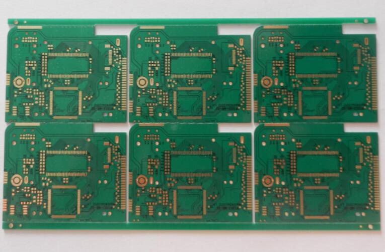
Copper-clad means to cover the area without wiring on the PCB board with copper foil and connect it to the ground wire to increase the ground wire area, reduce the loop area, reduce the voltage drop, and improve the power efficiency and anti-interference ability. In addition to reducing the impedance of the ground wire, copper coating also has the functions of reducing the cross-sectional area of the loop and enhancing the signal mirror loop. Therefore, the copper coating process plays a very critical role in the PCB process. Incomplete, truncated mirror loops, or incorrectly positioned copper layers often cause new interference and negatively affect the use of the circuit board.
DPC substrate preparation process flow
DPC substrate structure
Comparison of Copper Cladding Process and Thick Film Process
project
Copper Cladding Process
Thick film process
Conductive circuit metal composition

Pure copper wire has the advantages of excellent performance, not easy to oxidize, and will not produce chemical changes over time.
Silver-palladium alloy has disadvantages such as easy oxidation, easy migration, and poor stability.
The bonding force of metal and ceramic
The bonding force in the PCB industry can reach 18-30 MPa, and the bonding strength of the Stone ceramic circuit board is 45 MPa. The bonding force is strong, it will not fall off, and the physical properties are stable.
Poor binding force will continue to age with the passage of application time, and the binding force will become worse and worse.
Line accuracy, surface flatness and stability
Using the etching method, the edge of the line is neat and has no burrs, very fine and high precision. The copper thickness of the ceramic circuit board of Stone is customized between 1μm and 1mm, and the line width and line diameter can be 20μm.
Using the printing method, the product is relatively rough, and the edges of the printed circuit are prone to burrs and nicks. The thickness of the copper coating is less than 20μm, and the minimum line width and line diameter are up to 0.15mm.
Line location accuracy
Using the exposure and development method, the position accuracy is very high.
In screen printing, the accuracy will be deviated as the screen tension and printing times increase.
Line surface treatment
Surface treatment processes include nickel plating, gold plating, silver plating, OSP, etc.
Silver-palladium alloy.
LAM process and DPC process
In the LAM process, ceramic metallization uses a high-energy laser beam to state the ceramic and metal ions, so that the two are closely united to achieve the effect of growing together. The copper clad using LAM technology has the advantages of controllable copper layer thickness and easy control of graphic accuracy. The copper clad thickness of Stoneon ceramic circuit boards can be customized between 1μm and 1mm according to customer requirements, and the line width and line diameter can be 20μm. That is to say, with the application and deepening of science and technology in the laser field, the copper-clad technology in the printed circuit board industry can already achieve the effects of high ceramic and metal layer bonding and excellent performance through laser technology.
In the DPC process, the electroplating process is used. The ceramic metallization generally uses a sputtering process to form an adhesion layer made of chromium or titanium and a seed layer made of copper on the ceramic surface. The adhesion layer can increase the metal circuit. The copper seed layer acts as a conductive layer.