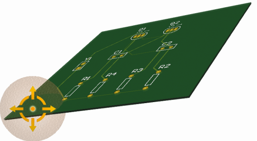
PCB design entry inspection PCB board design: can design PCB, and allows us to define many types of design rules to ensure the integrity of our PCB design. Typically, we establish design rules at the beginning of the design process, and then use these rules to verify and revise the design standards after the design process ends.
In the earlier tutorial guide, we checked the routing design rules and added a new width constraint rule. We also noticed that there are already some rules created by PCB Board EizardWizard.
In order to verify that the layout of the circuit board complies with the design rules, we will perform a design rule check (DRC):
1. Select Design>>Board Layers & Colors (shortcut key: L) and ensure that the Show button in the DRC Error Markers option in the System Colors section has been enabled (checked) to ensure that the DRC error markers are displayed.
2. Select Tools-Design Rule Check (shortcut keys: T, D). Ensure that both real-time and batch design rule checks in the Design Rule Checker dialog box are configured. Click on one of the categories, such as Electrical, and you can see all the rules belonging to that category.

3. Keep all options at their default values and click the Run Design Rule Check button. DRC starts to run, and the report file Multivibrator.DRC is opened. The error result will also be displayed in the information panel. Click to enter the PCB file and we will see that the pad of the transistor is highlighted in green, indicating a violation of the design rule.
4. By looking at the error report list in the information panel, it lists any violations of the rules that occurred in the PCB design. Note that there are four types of violation rules listed in the removal constraint rules. The details show that transistors Q1 and Q2 violate the 13mil minimum safety distance rule.
Double-click the error in the Messages panel to jump to the corresponding position in the PCB.
Usually, we will set our safety distance rules before wiring, taking into account the wiring technology and the physical performance of the equipment. Let us analyze the error, and then check the current safety distance design rules again and decide how to solve this situation.
In order to find the true minimum safety distance between two transistor pads, the following steps are taken:
1. Select the PCB file, position the cursor on a transistor, and press the PAGE UP key to enlarge the view image.
2. Select Reports-Measure Primitives (shortcut keys: R, P). The cursor will change to a cross-shaped character guideline.
3. Position the cursor in the middle of the pad on the left side of the transistor, and click or press ENTER. Because the cursor is over two pads and the wiring connecting it, a menu will pop up to let the user select the desired object. Select the pad of the transistor from the pop-up menu.
4. Once again, position the cursor in the middle of the transistor and click or press ENTER. Select the pad of the transistor from the pop-up menu. An information box showing the minimum distance is opened, showing that the minimum distance between the edges of the two pads is 10.63mil.
5. Close the information dialog box, right-click or press ESC to exit the measurement mode, and then use the shortcut keys of V and F to rescale the file.
Let us look at the current safety distance design rules:
Select Design-Rules (shortcut keys: D, R) from the menu to open the PCB Rules and Constraints Editor dialog box. Double-click the Electrical category, and all electrical rules will be displayed in the right dialog box. Double-click the safety distance type, and then click on the safety distance rule. Click the "Clearance" rule to open it. The area at the bottom of the dialog box will contain a single rule indicating that the minimum safety distance of the entire PCB board is 13mil. The distance between the pads of the transistors is less than the safe distance, which is why when we run DRC, they appear to violate the rules.
Now that the minimum pad distance between two transistors is a little more than 10 mils, let us establish a design rule for transistors only, with a size of 10 mils.
1. In the design rule folder, select the safety gap type, right-click and select new rule to add a new safety gap constraint rule.
2. Click on the new safety clearance rule, Clearance_1. In the Constraints chapter on the result page, set the Minimum Clearance to 10 mil.
3. Click Advanced (Query), then click Query Helper to create a conditional search from Memberships Checks, or you can print it in the next conditional search for the first object (Figure 6-35).
HasFootprintPad('TO-92A','*') The asterisk indicates any pad named "TO-92A" in the package.
1. Keep the second object range as ALL, and click OK. Click Apply, and then click OK to close the PCB Rules and Constraints Editor dialog box.
2. Now, we can click the Run Design Rule Check button from the Design Rule Check dialog box (Tools-Design Rule Check). Re-run DRC, there will be no violation of the rules.
3. Save the completed PCB and project files.
Up to now, congratulations, you have completed the PCB layout and are ready to generate output files.