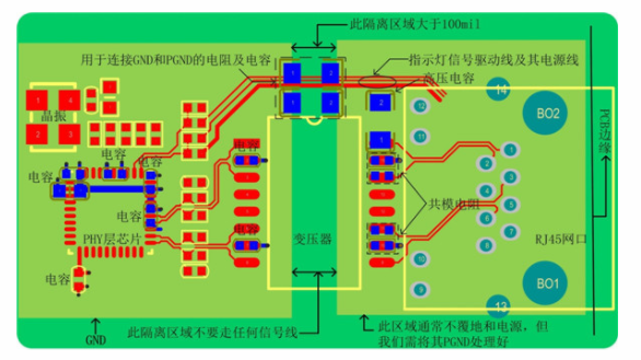
1. PCBA burn-in test standard and PCBA burn-in test method
The main purpose of the PCBA board aging test is to simulate the daily use environment of the product through the comprehensive effects of high temperature, low temperature, high and low temperature changes and electrical power, and expose the defects of PCBA, such as poor soldering, component parameter mismatch, and debugging process In order to eliminate and improve the caused failure, it will play a role in stabilizing the parameters of the non-defective PCBA board.
PCBA aging test standard
1. Low temperature work
After placing the PCBA board at a temperature of -10±3°C for 1h, under this condition, the rated load should be carried. Under the conditions of 187V and 253V, all programs should be powered on and the program should be correct.
2. High temperature work
After putting the PCBA board at 80±3 degree Celsius/h, under this condition, with load, under the conditions of 187V and 253V, power on and run all the programs. The program should be correct.

3. High temperature and humidity work
Put the PCBA board at a temperature of 65±3°C and a humidity of 90-95% for 48 hours and run the programs with a rated load. The programs should be correct.
PCBA aging test method
1. Put the PCBA board at ambient temperature into the heat aging equipment at the same temperature, and the PCBA board is in operation.
2. Reduce the temperature in the equipment to the specified temperature value at a specified rate. When the temperature in the equipment is stable, the PCBA board should be exposed to low temperature conditions for 2 hours.
3. Raise the temperature in the equipment to the specified temperature at a specified rate. When the temperature in the equipment is stable, the PCBA board should be exposed to high temperature conditions for 2 hours.
4. Reduce the temperature in the equipment to room temperature at a specified rate, continue to repeat until the specified aging time, and perform a measurement and record on the PCBA board according to the specified aging time.
2. How can PCBA assembly achieve reliability design
Stress-sensitive devices such as BGA, chip capacitors, and crystal oscillators are easily damaged by mechanical or thermal stress. Therefore, the design should be placed in a place where the PCB is not easily deformed, or reinforced design, or appropriate measures to avoid.
(1) The stress-sensitive components should be placed as far away as possible from the places that are prone to bending during PCB assembly. In order to eliminate the bending deformation during the assembly of the daughter board, the connector that connects the daughter board with the mother board should be placed on the edge of the daughter board as much as possible, and the distance from the screws should not exceed 10mm.
For another example, in order to avoid BGA solder joint stress cracking, it is necessary to avoid placing the BGA layout in a place that is prone to bending during PCB assembly. The poor design of BGA can easily cause its solder joints to crack when holding the board with one hand.
(2) Reinforce the four corners of the large-size BGA.
When the PCB is bent, the solder joints at the four corners of the BGA receive the greatest force and are most likely to crack or break. Therefore, strengthening the four corners of the BGA is very effective in preventing the cracking of the corner solder joints. Special glue should be used for strengthening, or patch glue can be used for strengthening. This requires space for component layout, and the reinforcement requirements and methods should be indicated on the process documents.
The above two suggestions are mainly considered from the design aspect. On the other hand, the assembly process should be improved to reduce the generation of stress, such as avoiding the use of supporting tools for holding the board with one hand and installing screws.
Therefore, the design of assembly reliability should not be limited to the improvement of the layout of the components. The more important thing should be to reduce the stress of the assembly-adopt appropriate methods and tools, strengthen the training of personnel, and standardize the operation actions. Only in this way can the assembly stage be resolved. The problem of solder joint failure.