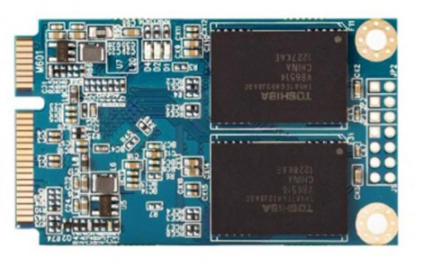
Electrostatic discharge (ESD) is the rapid discharge of voltage potential into the PCBA. The components that are sensitive to electrostatic discharge (ESDS) depend on the assembly situation. The magnitude of the current generated by the electrostatic discharge will determine whether the static current is an electrical overload (EOS) (ie, Electrical Overstress) or a complete failure. Before the PCBA reaches the control point of the qualification inspection process, any circuit protection design, and proper assembly and operation must have been completed.
ESD Electrostatic Discharge Marking and Marking-Prevention of Electrical Overload (EOS) and Electrostatic Discharge (ESD) Hazards
The electrical overload hazard is caused by undesirable electrical energy, caused by factors such as: spikes in electrical pulses that occur when using soldering irons, solder suction devices, test instruments, and other electrical devices.

Certain PCBA components are very sensitive to EOS damage. Similarly, changes in a particular device or a family of device series may each exhibit different degrees of EOS sensitivity. The degree of such sensitivity in a particular device is directly related to the PCBA manufacturing technology used.
The hazard of EOS is usually difficult to distinguish from the hazard caused by ESD. Therefore, if it is confirmed that EOS is the cause of destroying the device or degrading the device, the possibility of ESD must also be investigated.
Where sensitive components are handled, precautions should be taken to prevent component damage. Incorrect and careless operation is the cause of obvious EOS/ESD damage to components and PCBA.
When handling ESDS components, the device should be carefully inspected to confirm that it is unlikely to cause spikes. Studies have shown that the spike level is less than 0.5V as qualified. However, as the number of components that are particularly sensitive to ESD increases, it is required that soldering irons, tin suction devices, testing instruments and other direct contact equipment must not have spikes greater than 0.3V.
Static charges are generated when the non-conductive materials are separated, (for example, when the plastic bag is picked up or opened, when the plastic-soled shoes are separated from the carpet, etc.), friction occurs between the particles of the synthetic fabric, or use When using plastic solder removers, electrostatic charges are generated. Even when air molecules ejected from a gas nozzle collide with each other under suitable conditions, electrostatic discharge can be generated.
Destructive electrostatic charges are usually caused when they are close to a conductor (for example, human skin), and discharge sparks pass between adjacent conductors.
When a person with electrostatic potential energy touches the PCBA, electrostatic discharge will occur. When the electrostatic discharge reaches the components sensitive to static electricity through the conductor pattern, the components will cause PCBA damage. Even when the electrostatic discharge is too low to be felt (less than 3500V), it will still damage the ESDS components.
PCB factories should understand the basic range of sensitivity of certain components that are susceptible to EOS/ESD damage