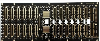
The traditional printed circuit board (PCB) consists of a non-conductive substrate material (usually a glass fiber epoxy structure), which is paired with a layer of conductive elements (such as copper) on one or both sides (single-sided or double-sided). Electronic components are placed on the circuit board and soldered in place, connected by drilling or STM components. One or both sides of the circuit board can be used to mount components.
Due to the physical properties of these PCBs, the size of a particular circuit or application may result in the need for a large circuit board, or even the use of multiple boards. This is the emergence of technology and manufacturing technology that allows the manufacture of multilayer boards, and is a major leap in the application of electronic products.
Multi-layer PCB advantages
Application circuit boards for multilayer printed circuits provide circuit board design engineers and product developers with many strategic advantages:

Space requirements-Creating a multi-layer printed circuit board design means that the advantages of this technology can greatly save space in the product. Considering that adding layers only slightly increases the thickness of the resulting board (depending on the number of layers), the benefits relative to larger single-sided or double-sided panels may be considerable. This is essential for modern electronic equipment.
Weight-Just like the space advantage, combining the component layers into a single multi-layer card can provide circuit functions, and only a small part of the weight is better than the existing technology. Think about the advantages of using it in personal electronics, laptops, and flat-screen TVs.
Reliability-The construction of multi-layer boards helps to improve reliability and consistency. Disadvantages of multi-layer PCBs
Just as important as multilayer boards is the ability to develop high-performance, compact electronic devices, such as smart phones, military equipment, aviation instruments, etc., trade-offs need to be considered when developing and using:
Cost-this is the primary consideration. With the special equipment required to manufacture multilayer PCBs, manufacturers must pass on this cost to customers, making PCBs more expensive than traditional circuit boards. Fortunately, with the increase in demand and the development of technology, this gap has been greatly reduced. Design tools-Creating detailed technical designs for manufacturers means that design engineers and layout technicians must transition to complex software to aid the design and manufacturing process. This requires training and a learning curve for designers. Replacement-Due to the structure and complexity of multi-layer PCBs, repairing faulty boards can be very troublesome if possible. In most cases, the failed circuit board causes the need to replace it instead of trying to repair it. Precautions for the manufacture of multilayer PCBs
The production of multi-layer circuit boards is not available from all PCB manufacturers. As the percentage of circuit boards required to design multiple layers increases, the number of manufacturers is expanding. Although the process is relatively simple, it requires specialized equipment and attention to detail. With the improvement of quality, efficient production also requires technical training.
The manufacturing process includes constructing layers of conductive materials such as copper foil, core material and prepreg layers, clamping them together, heating and applying pressure at high temperatures to laminate the layers together. Heating can melt and solidify the prepreg material, and pressure can remove air pockets that may affect the integrity of the circuit board.
These processes require specialized equipment and a significant commitment to operator training, not to mention economic considerations. This explains why some manufacturers are slower to enter the multi-layer manufacturing market than others.
Technology that supports multi-layer PCB design
An important development to be able to create and integrate multilayer boards into many industries and products is the creation of extremely complex software tools for use by design engineers, layout experts and manufacturers.
PCB design software promotes computer-aided design (CAD), enabling circuit designers to quickly increase efficiency, find errors or problem areas, and generate documents for manufacturers that are unlikely to be problematic for manufacturers. It can even analyze whether there is missing or incorrect content in the design file, avoiding traditional back and forth communication when creating problems or problems.
Design for Manufacturing (DFM) applications assist designers and manufacturers to verify the manufacturability of the final design through analysis functions. If there is no DFM tool, the PCB design can be manufactured to the manufacturer, finding that the PCB will be impractical, costly, and even impossible to build as designed.
Computer Aided Manufacturing (CAM manufacturers use software to verify and automate the actual manufacturing process.
These complex tools combine to make multi-layer PCB design and manufacturing more efficient, simplifying the process flow from start to finish. The result is a more reliable, lower-cost multilayer board, and improved project schedules.