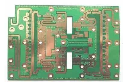
PCBA welding and heating process often produce a large temperature difference. Once this temperature difference exceeds the standard, it will cause poor welding. Therefore, we must control this temperature difference during operation. The thermal design of PCBA is constructed by many parts, and each part has different functions. We still need to understand.
PCBA processing-PCBA board thermal design structure and its structural characteristics
If this temperature difference is relatively large, it may cause poor soldering, such as the opening of the QFP pin, the rope suction; the tombstone and displacement of the chip component; the shrinkage and fracture of the BGA solder joint, etc.. For the same reason, we can change the heat capacity Solve some problems.
(1) Thermal design of heat sink pad

In the soldering of heat sink components, the phenomenon of less tin on the heat sink pad will be encountered, which is a typical application situation that can be improved by heat sink design.
For the above situation, you can use the method of increasing the heat capacity of the heat dissipation hole to design, connect the heat dissipation hole to the inner ground layer, if the ground layer is less than 6 layers, you can isolate the part from the signal layer as a heat dissipation layer, while reducing the aperture to the smallest Available aperture size.
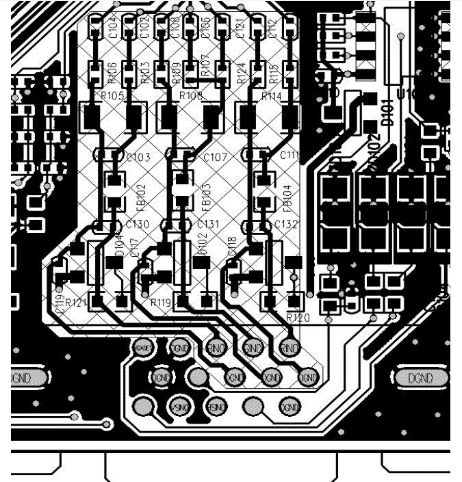
(2) Thermal design of high-power grounding jack
In some special product designs, the insertion hole sometimes needs to be connected to multiple ground/electric plane layers. Because the contact time between the pin and the tin wave during wave soldering is very short, it is often 2~3s, if the jack is The heat capacity is relatively large, and the temperature of the lead may not meet the welding requirements, forming a cold solder joint.
In order to avoid this situation, a design called star-moon hole is often used. The welding hole is separated from the ground/electrical layer, and a large current is realized through the power hole.
(3) Thermal design of BGA solder joints
Under mixed assembly process conditions, there will be a unique phenomenon of "shrinkage fracture" caused by unidirectional solidification of solder joints. The root cause of this defect is the characteristics of the mixed assembly process itself, but it can be wired through the corners of the BGA Optimize the design to make it cool slowly and improve it.
According to the experience provided by the case, the solder joints that generally undergo shrinkage and fracture are located at the corners of the BGA, and the heat capacity of the BGA corner solder joints can be increased or the heat transfer speed can be reduced to synchronize it with other solder joints or to cool afterwards. Cooling causes it to be broken under the BGA warping stress.
(4) Design of chip component pad
As the size of chip PCB components becomes smaller and smaller, there are more and more phenomena such as displacement, tombstone, and flipping. The occurrence of these phenomena is related to many factors, but the thermal design of the pad is an aspect that has a relatively large impact.
If one end of the pad is connected to a wider wire and the other end is connected to a narrower wire, the heating conditions on both sides will be different. Generally speaking, the pad connected to the wide wire will melt first (this is contrary to general expectations. It is generally believed that the pad connected to the wide wire will melt due to its large heat capacity. In fact, the wide wire becomes a heat source, which is related to the heating method of the PCBA board.) The surface tension generated by the first melting end may also displace the component. Even flip.
(5) The influence of wave soldering on the component surface
BGA:
Most of the pins of the BGA with a pin center distance of 0.8mm and above are connected to the circuit layer through vias. During wave soldering, heat will be transferred to the BGA solder joints on the component surface through the vias. According to the different heat capacity, some are not melted, some are semi-melted, and they are easy to break and fail under the action of thermal stress.
Chip capacitors:
Chip capacitors are very sensitive to stress and are susceptible to cracking due to mechanical and thermal stress. With the widespread use of wave soldering of trays, the chip PCB components at the boundary of the tray window are easily broken due to thermal stress.