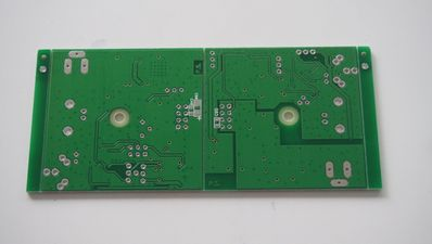
PCB design continues to be challenged by electronic products through the need for engineering boards to place components most effectively to meet the required functions and at the same time meet the product specifications that include the circuit board. Therefore, smaller components must be put together while avoiding the potential
In fact, preparations play an important role in PCB layout and design results. Starting with the most important requirements, you can help simplify the design process by identifying design constraints. The size and location of key components, including minimum and maximum tolerances, required components, and electrical requirements (including impedance factors and power requirements) can all be combined to create a set of initial constraints for the PCB design. It is also a good practice to create and save a collection of similar constraints and templates for subsequent designs or projects. Having time-proven templates can simplify the design of new boards or the upgrade of existing PCBs. Once the constraints are set and understood, it makes the details less error-prone, thus saving time and money.
Circuit board layout technology can include strategies such as devices embedded in the inner layer of the PCB to reduce the size of the circuit board. This must be evaluated together with the manufacturer to verify whether these functions can be met in actual manufacturing.
1. Errors or lack of planning in PCB layout specifications may cause multiple problems:
Quality or functional issues of manufactured products that do not comply with regulations or designs may surface due to components and circuit paths that conflict with factors such as electromagnetic interference, current, track width, component size, and physical circuit board limitations. Circuit boards may not be manufactured in accordance with regulations, leading to decisions made back and forth between the designer and the manufacturer. This prolongs delivery time and increases costs. Worst case scenario-the engineer goes back to the "drawing board" to redesign manufacturability.

In practice, most PCBs are designed using CAD or other PCB design tools, and technicians are most familiar and familiar with it. In fact, once the design is completed, the manufacturer will use its own automated tools and sophisticated computer-aided manufacturing (CAM) manufacturing technology to manufacture the circuit board from the files or documents generated by the design tool. The two processes may not be completely synchronized during the processing, resulting in the circuit board may not produce the expected results, or may not be easy to manufacture, resulting in delays and increased costs.
2. How should PCB designers meet the needs of effective PCB layout?
Therefore, designers are motivated not only to generate a design, not only to consistently generate the required functions, but also to generate a layout point that can achieve efficient manufacturing at the required cost. Engineers need to understand the manufacturing process to a certain degree in order to understand how the manufacturing method reacts to its design. Multilayer boards and double-sided laminates or double-sided component placement designs can make layout
3.more critical in design for manufacturing (DFM).
In the manufacturing process of PCB manufacturers, the placement of components may be a tool that determines that the result is not the result expected by the designer due to automation. In many cases, the final product is acceptable and functional, but failure can also be an unexpected consequence.
The wiring of the circuit path can be changed during manufacturing and still produce a usable PCB, but it may also make the circuit board more difficult to install or repair than the original design.
Effective Before the prototype is created, the tool that PCB designers can use is DFM software. Such tools can analyze the designer's files and evaluate any issues or omissions related to manufacturing. Combining the use of PCB design tools and DFM applications is the best solution for designing the highest quality PCBs that will be functional and cost-effective.