According to the functional unit of the circuit.
When arranging all PCB components of the circuit, the following principles must be met:
(1) Arrange the position of each functional circuit unit according to the flow of the circuit, make the layout easy for signal flow, and keep the signal in the same direction as possible.
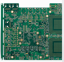
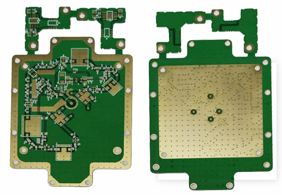
(2) Take the core component of each functional circuit as the center and lay out around it. The components should be evenly, neatly and compactly arranged on the PCB.
Minimize and shorten the leads and connections between components.
(3) Circuits operating at high frequencies should consider the allocation parameters between components. The general circuit should connect components in parallel as much as possible. In this way, it is not only beautiful, but also easy to install and weld, which is convenient for mass production.

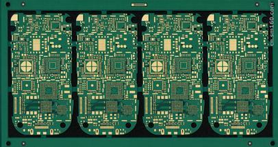
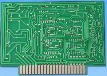
(4) PCB components are located on the edge of the circuit board, and the edge of the circuit board is generally not less than 2mm. The best shape of the circuit board is rectangular. The length and width are doubled to 3:2 or 4:3.
When the PCB size is larger than 200x150mm, the mechanical strength of the circuit board should be considered.
3. The center hole of the soldering board pad is slightly larger than the diameter of the device lead. If the weld plate is too large, it is easy to form a false weld. The outer diameter of the pad d is usually not less than (d + 1.2) mm, where D is the guide hole.
For high-density digital circuits, the minimum diameter of the pad is ideal (d + 1.0) mm.
Second, PCB and circuit anti-interference measures
The anti-jamming design of the printed circuit board is closely related to the specific circuit, and here is just an explanation of some common measures of the PCB anti-jamming design.
1. The design of the power line is based on the current of the printed circuit board, try to increase the width of the thick power line and reduce the loop resistance.
At the same time, the power line, ground line and data transmission direction are the same, which helps to enhance the anti-noise ability.
2. Ground wire design In the design of electronic products, grounding is an important method to control interference. If the grounding and shielding are combined correctly, most interference problems can be solved. The ground structure of electronic products is roughly systematic, shell (shielded), digital (logic) and analog.
The following points should be paid attention to in the ground wire design:
(1) Correctly choose single-point grounding and multi-point grounding. In low-frequency circuits, the working frequency of the signal is less than 1MHz, and the inductance between the wiring and the device has little influence. The circulation circuit formed by grounding has a great influence on interference, so it should be Use one-point grounding method. When the signal working frequency is greater than 10MHz, the ground impedance becomes very large. At this time, the ground impedance should be reduced as much as possible, and it should be used near multi-point grounding.
When the working frequency is 1~10mhz, if a small amount of grounding is used, the length of the grounding wire should not exceed 1/20 of the wavelength, otherwise, multi-point grounding should be used.
(2) The digital ground is separated from the analog place. There are high-speed logic circuits and linear circuits on the circuit board. They should be kept as separate as possible, and the ground wires of the two should not be connected to the ground wires of the power supply terminal respectively. Low-frequency circuits should try to use single points and be grounded. If the actual wiring is difficult, part of them can be connected and then grounded. The high-frequency circuit should be grounded at multiple points in series, the ground wire should be short and thick, and the surrounding high-frequency components should be filmed with a large area of grating as much as possible.
Try to increase the grounding area of the linear circuit.
(3) The grounding wire forms a closed loop. A PCB grounding system composed of only digital circuits is designed. By closing the grounding wire, the anti-noise capability can be significantly improved. The reason is: the printed circuit board has many integrated circuit components, especially in the case of components with high power consumption, due to the thickness of the ground wire, a large potential difference will be generated on the ground, resulting in anti-noise. If the ground wire is formed The loop will reduce the potential difference and improve the anti-noise ability of electronic equipment.