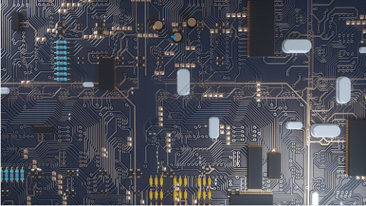
Several issues that should be paid attention to in the PCB proofing process:
1. Electromagnetic compatibility Electromagnetic compatibility (EMC) is a comprehensive subject, mainly studying electromagnetic interference and anti-interference issues. Electromagnetic compatibility refers to verification that electronic equipment Or system, to achieve no interference between equipment and equipment, system and system, requires cooperative work and reliability. Electromagnetic compatibility (EMC) includes two aspects: the electromagnetic radiation of the product and the electronic products with good anti-electromagnetic interference ports must consider the electromagnetic compatibility problem, can not produce electromagnetic radiation interference with other electronic equipment, and have lower electromagnetic sensitivity. Resist the specified electromagnetic interference. Electromagnetic interference is the result of electromagnetic disturbance, which will degrade the performance of electronic equipment, transmission channels, systems and printed circuit board components.

As the basic part of electronic equipment, printed boards use the same electric and magnetic fields. There are electromagnetic compatibility problems with electricity and magnetic fields, especially the large number of digital circuits and high-speed logic circuits in modern electronic equipment. The signal transmission speed is greatly improved, which also increases Causes of electromagnetic radiation and electromagnetic interference factors
Therefore, considering the electromagnetic compatibility issue is an important part of PCB design.
Second, the design to suppress electromagnetic interference on the printed circuit board
Due to the increase in the density of electronic devices and circuits on the PCB and the increase in signal frequency, the problems of electronic fraud (electromagnetic compatibility) and negative (electromagnetic interference) will inevitably be introduced. External conduction interference and radiation interference have no effect on the circuit on the PCB. In fact, taking correct measures in the design can often play a role in anti-interference and suppression of emission.
In PCB design, first, select the appropriate type of printed board (board and layer) according to actual needs, and then determine the position of the components on the board, and then layout, design the ground line and signal line.
2.1, the choice of printed circuit boards: printed circuit boards are divided into single-sided, double-sided and multi-layer panels. Single-sided and double-sided boards are usually used for low- and medium-density wiring circuits and fewer integrated circuits. Multilayer boards are suitable for high-speed digital circuits with high-density wiring and highly integrated chips. From the perspective of electromagnetic compatibility, multi-layer boards can reduce the electromagnetic radiation of the circuit board and improve the anti-interference ability of the circuit board. Because in the multi-layer board, you can set up special power layers and layers, so that the distance between the signal line and the ground line is only the distance between the cable printed circuit boards.
In this way, the loop area of all signals on the board can be minimized, thereby effectively reducing differential mode radiation.
2.2PCB component layout:
The design of the printed circuit board is not only simply to connect various components with printed wires, but more importantly, the characteristics and requirements of the circuit should be considered, the component L should be placed correctly, and the circuit unit of the PCB component and connected to each other should be close to the layout. .
Reduce wiring and wiring length between components, reduce radiation and interference.
2) According to the operating frequency of the circuit or the switching speed of the relatively high-low partition layout of the device, the operating frequency of the terminal circuit is reduced in order from the i/0 terminal. In the higher frequency region, the high-speed oscillating device should not be close to the working/0 terminal. 3) Electromagnetic radiation-prone components (such as clocks, oscillators, etc.) should be kept away from electromagnetic sensitive devices or wiring, and electromagnetic shielding measures should be taken if necessary.