For the most basic PCB, the PCB components are concentrated on one side and the wires are concentrated on the other side, because they can only be wired, so we call this PCB a single panel.
Both sides of the double-sided board can be wired, so the wiring area is twice as large as that of the single-sided board, which is suitable for more complicated circuits. For simple circuits such as radios, single or double panels can be used. However, with the development of microelectronics technology, the complexity of the circuit has been greatly improved, and higher requirements have been placed on the electrical performance of the PCB. If a single-sided or double-sided board is used, the circuit volume will be very large. Brings great difficulties, in addition, electromagnetic interference between lines is not easy to deal with
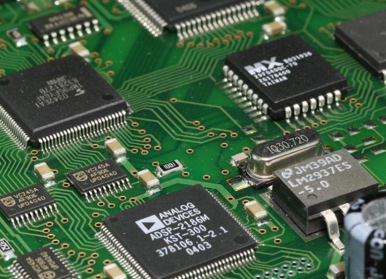
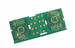
So there is a multi-layer board (the number of layers represents several independent wiring layers, usually an even number).
The advantages of multi-layer boards: high assembly density, small size, shorten the connection between electronic components, improve signal transmission speed, facilitate wiring, apply to high-frequency circuits, increase grounding layers, and make signal lines form a constant low impedance. The shielding effect is very good.

However, the more layers, the higher the cost, the longer the processing cycle, and the more troublesome quality testing is. Our commonly used computer boards usually use four-layer or six-layer circuit boards, but now there are more than 100 practical printed circuit boards.
The difference between the six laminates and the four laminates is that there are two additional internal signal layers between the ground layer and the power layer, which are thicker than the four-layer board. Multilayer boards are actually laminated and glued through several etched single or double panels. The double panel is easy to distinguish, except for the lines on both sides, all other parts are transparent. For four-layer and six-layer boards, because the layers in the PCB are very tightly integrated, if the boards have corresponding marks, there is no good way to distinguish them.
PCB copy board design experience sharing
No matter what software is used, PCB design has a general program. In order to save time and energy, I will introduce it according to the production process (because the Protel interface style is similar to Windows Windows Close, the operating habits are similar, and it has a powerful simulation function. More people will be explained through this software). Schematic design is a preparatory work. It is often seen that beginners directly draw the PCB board in order to save it directly, so that it will not be rewarded. As far as the simple board is concerned, if you are proficient in the process, you may wish to skip it. But for the beginners must follow the process, so that on the one hand you can develop good habits, on the other hand, the complex circuit is the only way to avoid mistakes. When drawing the schematic, the hierarchical design should pay attention to the individual files that are ultimately connected to the whole, which is also very important for future work. Due to the difference in software, some software seems to be connected to the actual unconnected (electrical performance) situation. If you have not used the relevant test tools to detect, in case there is a problem, please wait for the circuit board to be ready to find that it is too late. Therefore, repeated emphasis on the importance of ordering, I hope it can attract everyone's attention. The schematic is based on the design of the project, as long as the electrical connections are correct, there is nothing to say.
Let us focus on the issues in the specific board-making plan.
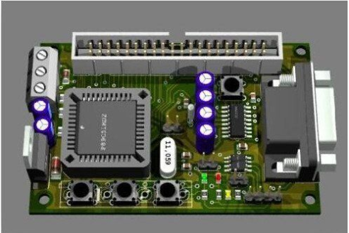
1. Making physical borders Closed physical borders are used for future component layout. Wiring is a basic platform and a constraint on automatic layout. Otherwise, the schematic diagram of the component will be overwhelmed. But you must pay attention to the accuracy here, otherwise you may encounter big troubles in the future installation problems. It is best to use an arc shape for one corner, which can avoid scratching the workers by sharp corners and reduce the pressure at the same time.
In the past, one of my products always showed the PCB board breakage of the shell of individual machines during transportation, rather than after the arc.
2. Introduction to Components and Networks It should be easy to draw a good border using components and networks, but there are often problems here. We must carefully solve the errors one by one according to the prompts, otherwise more effort will be spent later.
The problems here generally include: unable to find the package form of the component, component network problems, unused components or pins, control prompt 2 These problems can be solved quickly.
3. Component layout Component layout and wiring have a great impact on product life, stability, and electromagnetic compatibility. Special attention should be paid to it.
Generally speaking, there should be the following principles:
(1) Placement sequence First place the components related to the fixed position of the structure, such as power sockets, indicator lights, switches, connectors, etc. These devices are locked by the software lock function after use to avoid misoperation. Re-place special components on circuits and large components, such as heating elements, transformers, ICS, etc.
Place the small device last.
(2) Pay attention to the layout of heat dissipation components and pay special attention to heat dissipation issues.
For high-power circuits, those heating elements such as power tubes, transformers, etc. should be distributed as much as possible, easy to dissipate heat, not concentrated in one place, and high capacitors should not be too close to avoid premature aging of the electrolyte.
4. wiring
Wiring principles The learning of walking wires is very deep. Everyone has their own experience, but there are still some common principles. High-frequency digital circuit wiring, short some good high-current signals, high-voltage signals and small signals should be separated (isolation distance and withstand voltage, usually 2KV time plate to 2mm distance, which is also increased on the scale, for example, To withstand the 3KV pressure test, the distance between the high and low voltage lines should be above 3.5mm, in many cases to avoid crawling, and slotting between the high and low voltages between the printed circuit boards.)