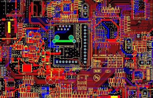
The correct installation and layout of components on PCB is a very important step to reduce welding defects. The layout of components should be far away from the area with large deflection and high stress area as far as possible, and the distribution should be as uniform as possible. Especially for components with large thermal capacity, the use of oversized PCB should be avoided as far as possible to prevent warpage. Poor layout design will directly affect the producibility and reliability of PCB. Next, let's understand what requirements are required for the placement of components.

PCB layout
PCB layout requirements for component layout
Components close to the edge of printed circuit board is not conducive to automatic assembly, mechanical stress concentration, easy damage in the process of turnover, metallized hole and pad are easy to be damaged. It is not allowed to place comp PCB layout requirements for component layout
onents within 5mm from the process edge, clamping edge or printed circuit board edge.
When placing components close to the edge of printed circuit board, the long side of components shall be parallel to the edge of printed circuit board. The chip ceramic capacitors near the edge of panel, screw and socket are easy to fail after high temperature aging or use for a period of time.
A certain maintenance space should be reserved around the large components to facilitate the operation of the heating head of the repaired equipment. When placing components close to the edge of large components, the long side of components shall be parallel to the edge of components.
Key and valuable components, such as high stress concentration areas near connector, mounting hole, slot, panel cutting, notch, corner and fastener, are easy to cause solder joint fatigue or solder joint fracture.