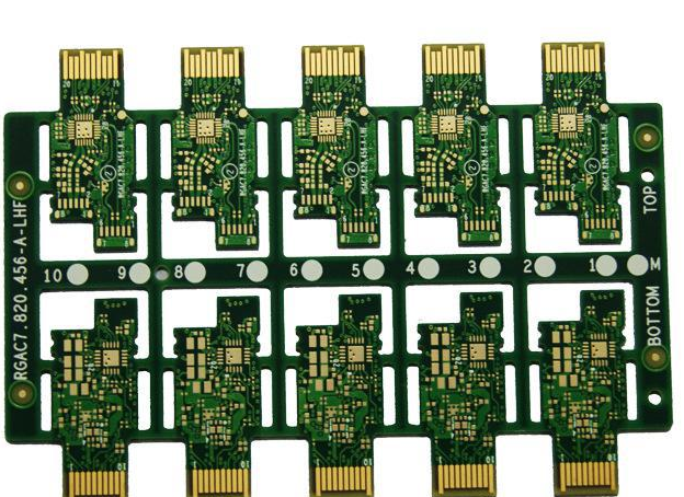
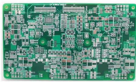
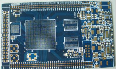
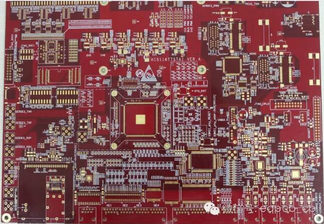
The PCB board is made up of layers of copper foil circuits, and the connection between the different circuit layers is via vias. This is because the current manufacturing of PCB board proofing uses drilled holes to connect to different The circuit layer, the purpose of connection is to conduct electricity, so it is called a via. In order to conduct electricity, a layer of conductive material (usually copper) must be plated on the surface of the hole, so that the electrons can be in different Move between the copper foil layers, because the surface of the original drilled hole is only non-conductive.

Generally, there are three types of PCB vias(Via) that we often see, which are described as follows:
Through hole: Plating Through Hole referred to as PTH
This is the most common type of via hole. You only need to pick up the PCB and face the light, the hole that can see the bright light is the "through hole". This is also the simplest type of hole, because when making it, you only need to use a drill or a laser to directly drill the PCB board, and the cost is relatively cheap. Although through holes are cheap, they sometimes use up more PCB space. For example, we have a six-story house. I bought its third and fourth floors. I want to design a staircase inside and only connect between the third and fourth floors. For me, the space on the fourth floor. Invisibly, the original staircase connecting the first floor to the sixth floor used up some space.
Blind Hole: Blind Via Hole (BVH)
The outermost circuit of the PCB is connected to the adjacent inner layer with a plated hole. Because the opposite side cannot be seen, it is called a "blind hole". In order to increase the space utilization of the PCB circuit layer, a "blind via" process has emerged. This production method requires special attention to the depth of the drilling (Z axis) to be just right. You can drill holes in the circuit layers that need to be connected in advance in the individual circuit layers, and then glue them together, but it requires more precise positioning. And counterpoint device. Take the above example of buying a building. A six-story house has only the stairs connecting the first floor and the second floor, or the stairs connecting the fifth floor to the sixth floor, which are called blind holes.
Buried via: Buried Via Hole (BVH)
Any circuit layer inside the PCB is connected but not connected to the outer layer. This process cannot be achieved by drilling after bonding. It must be drilled on the individual circuit layers. After the inner layer is partially bonded, it must be electroplated before it can be fully bonded. Compared with the original "through hole" and "Blind holes" take more time, so the price is the most expensive. This process is usually only used for high-density (HDI) circuit boards to increase the usable space of other circuit layers. Take the example of buying a building above. A six-story house only has stairs connecting the third and fourth floors, which are called buried holes.