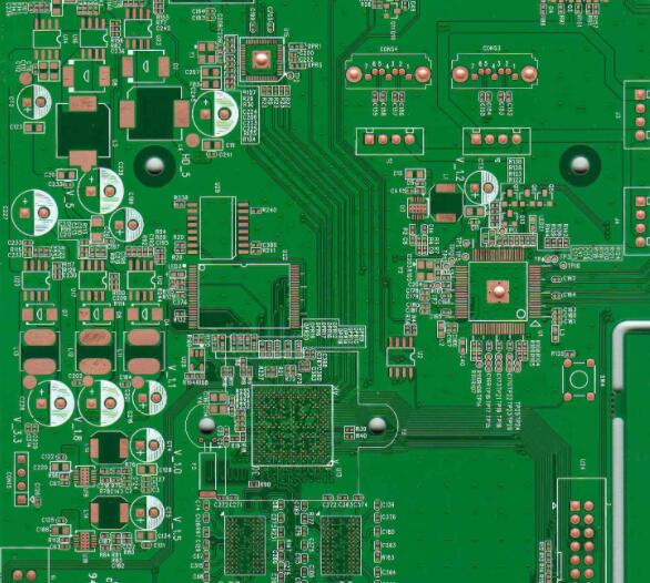
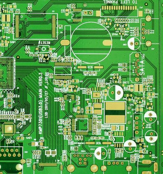
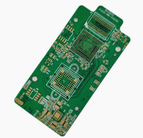
Shen'an PCB circuit board production automatic detection technology
With the introduction of surface mount technology, the packaging density of circuit boards has increased rapidly. Therefore, even for the low-density, general-quantity circuit board processing, the automatic inspection of circuit board production is not only basic, but also economical. In complex circuit board processing and inspection, two common methods are the needle bed test method and the double probe or flying probe test method.
1. Needle bed test method
This method is connected to each inspection point on the PCB processing by a probe with a spring. The spring makes each probe have a pressure of 100-200g to ensure good contact of each detection point. Such probes are arranged together and are called "beds of needles". Under the control of the detection software, the detection points and detection signals can be programmed, and the inspector can get the information of all the test points. In fact, only the probes of the test points that need to be tested are installed. Although it is possible to use the bed-of-needle test method to test on both sides of the printed circuit board at the same time, when designing the printed circuit board, all inspection points should be made on the soldering surface of the circuit board production. The needle bed tester is expensive and difficult to repair. According to the specific application of the needle, the probes in different arrangements are selected.

A basic general-purpose grid processor consists of a drilled board with a pin center spacing of 100, 75, or 50 mils. The pins act as probes and use electrical connectors or nodes on the circuit board to make direct mechanical connections. If the pads on the circuit board are matched with the test grid, then the polyester film perforated in accordance with the specification will be placed between the grid and the printed circuit board to facilitate the design of specific detection. Continuity detection is achieved by accessing the end points of the grid (which have been defined as the x-y coordinates of the pad). Since every network on the printed circuit board is tested for continuity. In this way, an independent circuit board production inspection is completed. However, the proximity of the probe limits the effectiveness of the bed-of-needle test method.
2 Double probe or flying probe test method
Flying probe tester does not depend on the pin pattern installed on the fixture or bracket. Based on this system, two or more probes are mounted on a tiny magnetic head that can move freely on the x-y plane, and the test points are directly controlled by CADI Gerber data. The dual probes can move within a distance of 4 mils from each other. The probes can move independently, and there is no real limit to how close they are to each other. The tester with two arms that can move back and forth is based on the measurement of capacitance. The printed circuit board is pressed tightly and placed on the insulating layer on a metal plate as the other metal plate of the capacitor. If there is a short circuit between the lines in the circuit board production, the capacitance will be larger than at a certain point. If there is an open circuit, the capacitance will become smaller.
Circuit board processing and testing speed is an important criterion for selecting a tester. The bed of needle tester can accurately test thousands of test points at a time, while the flying probe tester can only test two or four test points at a time. In addition, the needle bed tester may only cost 20-305 for a single-sided test, depending on the complexity of the circuit board processing, while the flying probe tester requires Ih or more time to complete the same evaluation. Shipley (1991) explained that even if high-volume circuit board manufacturers consider the mobile flying probe test technique to be slow, this method is still a good choice for lower-volume complex circuit board manufacturers.
For the bare board test of PCB processing, there are special test instruments (Lea, 1990). A more cost-optimized method is to use a general-purpose instrument. Although this type of instrument is initially more expensive than a dedicated instrument, its initial high cost will be offset by the reduction in individual configuration costs. For general grids, the standard grid for boards with pin components and surface mount equipment is 2.5mm. At this time, the test pad should be greater than or equal to 1.3mm. For the grid of Imm, the test pad is designed to be larger than 0.7mm. If the grid is small, the test needle is small, brittle, and easily damaged. Therefore, it is best to choose a grid larger than 2.5mm. Crum (1994b) stated that the combination of a universal tester (standard grid tester) and a flying probe tester can make the detection of high-density PCBs both accurate and economical. Another method he suggested is to use a conductive rubber tester, which can be used to detect points that deviate from the grid. However, the height of the pads that are processed by the hot air leveling of the circuit board is different, which will hinder the connection of the test points.