For PCB designers, we can not only consider the design and perfect requirements in the process of PCB design, there is a big constraint is the production process.
Good products are piled up under existing production conditions. Including PCB layer number, thickness, hole diameter, line width, wire spacing, copper thickness and other basic parameter requirements; also includes special requirements such as plate type, surface treatment, special processing, etc. Generally, when PCB is processed, it is divided into test proofing processing and final forming batch product processing. For PCB designers, it is of practical significance and need to strictly abide by the process requirements of batch product processing.
For the manufacturing related process requirements, the basic importance is the line width, line spacing and aperture. That is, how thin the line width and how large the hole can be processed by the processing plant. If the line width does not meet the requirements in the design, it can not be processed correctly if it is too thin. Line width and line spacing also affect the clarity of the text pattern on the silk screen layer. If the aperture is too small, there is no corresponding bit support. The drill size corresponding to the hole diameter also affects the tolerance of various types of plate shear, such as mechanical hole, mounting hole, etc.

Line width, line distance and aperture setting of PCB
Precautions for PCB line width distance and aperture rule setting
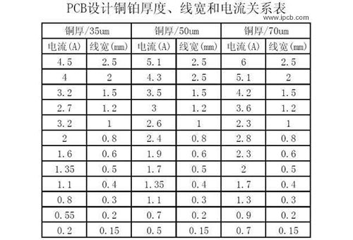
In PCB design, the line width and line spacing of 4 mil can be supported by batch processing. That is, the wiring width must be greater than 4mil, and the distance between two lines should be greater than 4mil. Of course, it's just the limit of line width and line spacing. In the actual work, the line width should be defined as different values according to the design needs. For example, the definition of power network is wider and the definition of signal line is more detailed.
These different requirements can define different network width values in the rules, and then set the rule application priority according to the importance. Similarly, for line spacing, define the electrical safety distance between different networks in the rule page design - Rules - Electrical - clearance, including line spacing.
There is another special case. For components with high-density pins, the spacing between pads in the device is generally very small, such as 6mil. Although it meets the manufacturing requirements of line width or spacing greater than 4mil, it may not meet the requirements of regular design as a PCB design.
If the safety spacing of the whole PCB is set to 8mil, the spacing of component pads obviously violates the rule setting. Violations are always highlighted in green during rule checking or online editing. This violation obviously does not need to be handled, we should fix the rule settings to eliminate the green highlight. In the original method, query language is used to define different security distance rules for this device, and set it as high priority. In the new version, simply check the option to ignore pad to pad clearance within a footprint. As shown in the figure below.
It's very easy to check with this option. It is not necessary to use the query statement incomponent ('u1 ') as before, and then set the safe distance as 6mil, and set it as the priority of spacing, via and aperture: 0.3mm (12mil).
The via diameter shall not be less than 0.3 mm (12 mil), and the single side of pad shall not be less than 6 mil (0.153 mm), and larger than 8 mil (0.2 mm) is not limited (see Figure 3). This is very important and must be considered in design.
Via hole to hole spacing (hole edge to hole edge) should not be less than 6mil and more than 8mil, which is very important and must be considered in design.
The size of plug-in hole depends on your component, but it must be larger than your component pin. It is suggested that the size of 0.6 component pin should be less than 0.8, in order to prevent machining tolerance from making it difficult to insert.
One side of outer ring of plug-in hole (PTH) pad should not be less than 0.2mm (8mil). Of course, the larger the better (as shown in Figure 2), this is very important and must be considered in design.
The hole to hole spacing (hole edge to hole edge) of plug-in hole (PTH) should not be less than 0.3mm. Of course, the larger the better (as indicated in Figure 3), this is very important and must be considered in design.
508mm (20MIL) from pad to contour line.
One side of SMD window opening should not be less than 0.1mm (4mil).
The width of a character cannot be less than 0.153mm (6mil) and the height cannot be less than 0.811mm (32mil). The relationship between the ratio of width to height is 5, that is to say, the width of a character is 0.2mm, and the height of a character is 1mm.
The distance between non-metallic slot holes should not be less than 1.6 mm, otherwise it will greatly increase the difficulty of edge milling.
There is no gap in the assembly, and there is a gap in the assembly. The clearance of the assembly with clearance should not be less than 1.6 (plate thickness is 1.6) mm, otherwise it will greatly increase the difficulty of edge milling. The size of the working plate depends on the equipment. The gap of the seamless assembly is about 0.5mm, and the process side cannot be less than 5mm.