1. Stacking scheme 1: top, gnd2, pwr3, bottom
This scheme is the mainstream 4-tier solution in the industry. There is a perfect ground plane under the top, which is the wiring layer. When the layer thickness is set, the thickness of the core plate between the ground plane layer and the power plane layer should not be too thick, so as to reduce the distributed impedance of the power supply and ground plane and ensure the plane capacitance filtering effect.
2. Stacking scheme 2: top, pwr2, gnd3 and bottom
If the main component surface is designed at the bottom layer or the key signal line is at the bottom layer, the third layer should be arranged in a complete ground plane. When the layer thickness is set, the thickness of the core plate between the ground plane layer and the power plane layer should not be too thick.
3. Stacking scheme 3: GND1, S2, S3, gnd4 / pwr4
This scheme is usually used in the design of interface filter board and backplane. Since there is no power plane in the whole board, GND and PGND are arranged on the layer and the fourth layer respectively. Only a small number of short wires are allowed in the surface layer (top layer). Similarly, we lay copper on the S02 and S03 wiring layers to ensure the reference plane and control stack symmetry of the surface wiring.

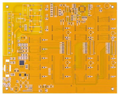
stacking of Multilayer PCB
Design scheme of six layer plate lamination
1. Stacking scheme 1: top, gnd2, S3, pwr4, gnd5 and bottom. This scheme is the mainstream 6-layer solution in the industry, with 3 wiring layers and 3 reference planes. The thickness of the core between layer 4 and layer 5 should not be too thick in order to obtain lower transmission line impedance. Low impedance can improve the decoupling effect of the power supply.
The third layer is the wiring layer. High risk wires such as clock lines must be laid in this layer to ensure signal integrity and resist EMI energy. The bottom layer is the second best wiring layer. The top layer is the wireable layer.
2. Stacking scheme 2: top, gnd2, S3, S4, pwr5 and bottom. When there are too many wires on the circuit board and the three wiring layers cannot be arranged properly, this stacking scheme can be adopted. There are four wiring layers and two reference planes in this scheme, but there are two signal layers between the power plane and the ground plane, and there is no power decoupling between the power supply plane and the ground plane.
Since the third layer is close to the ground plane, it is the wiring layer, and high-risk lines such as clock should be arranged. The first layer, the fourth layer and the sixth layer are the wiring layer.
3. Stacking scheme 3: top, S2, gnd3, pwr4, S5 and bottom. This scheme also has four wiring layers and two reference planes. The power plane / ground plane of this structure adopts a small spacing structure, which can provide lower power impedance and better power decoupling effect.
The top and bottom layers are poor wiring layers. The second layer near the ground plane is the wiring layer, which can be used to lay high-risk signal lines such as clocks. Under the condition of ensuring RF CO current path, layer 5 can also be used as the wiring layer of other high-risk signal lines. Cross wiring shall be used in layers 1 and 2, 5 and 6.
Design scheme of 8-layer laminate
1. Stacking scheme 1: top, gnd2, S3, gnd4, pwr5, S6, gnd7, and bottom. This scheme is the main layer selection scheme for the current 8-layer PCB in the industry, with 4 wiring layers and 4 reference planes. The signal integrity and EMC characteristics of this stacked structure are both good, and the decoupling effect of power supply can be obtained.
The top and bottom layers are EMI routable layers. Layer 3 and layer 6 adjacent layers are reference planes, yes, wiring layers. The third layer is the ground plane, so it is the routing layer. The thickness of the core plate between layer 4 and layer 5 should not be too thick in order to obtain a lower transmission line impedance, which can improve the decoupling effect of the power supply.
2. Stack scheme 2: top, gnd2, S3, pwr4, gnd5, S6, pwr7, and bottom. Compared with scheme 1, this scheme is applicable to the situation where there are many types of power sources and one power plane cannot handle it. The third layer is the wiring layer. The main power supply should be arranged in the fourth layer, which can be adjacent to the main ground.
In order to improve the decoupling effect of the power supply, the ground copper should be paved in the bottom layer. In order to balance PCB and reduce warpage, the top layer also needs to be covered with copper.
3. Stacking scheme 3: top, S2, gnd3, S4, S5, pwr6, S7 and bottom. This scheme has six wiring layers and two reference planes. The power supply decoupling characteristics of this stacked structure are very poor, and the EMI suppression effect is also very poor. The top and bottom layers are wiring layers with poor EMI characteristics. The second and fourth layers close to the ground plane are the wiring layers of clock lines, and cross wiring shall be adopted.
Layers 5 and 7 close to the power plane are acceptable wiring layers. This scheme is usually used in the design of 8-layer backplane with less chip devices. Since there are only sockets on the surface layer, the surface layer can be covered with copper in large area.