PCB secondary design and development, consider how to integrate the latest advanced technology into the product. These advanced technologies can be embodied in excellent product functions, but also in reducing product costs. The problem lies in how to effectively apply these technologies to products. There are many factors to consider. The time to market is one of the most important factors, and many decisions around the time to market are constantly updated. There are a wide range of factors that need to be considered, including product functions, design implementation, product testing, and whether electromagnetic interference (EMI) meets the requirements. It is possible to reduce the repetition of the design, but this depends on the completion of the previous work. Most of the time, it is easier to find problems in the later stages of product design, and it is more painful to make changes to the discovered problems. However, although many people know this rule of thumb, the actual situation is another scenario, that is, it is important for many companies to have a highly integrated design software, but this idea is often compromised by a high price. This article will explain the challenges faced by PCB secondary design and what factors should be considered when evaluating a PCB design tool as a PCB designer.

The following are several factors that PCB designers must consider and influence their decision:
1. Product function
A. The basic functions of the basic requirements of the cover, including:
a. Interaction between schematic and PCB layout
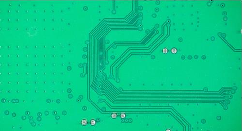
b. Wiring functions such as automatic fan-out wiring, push-pull, etc., and wiring capabilities based on design rule constraints
c. Precise DRC checker
B. The ability to upgrade product functions when the company is engaged in a more complex design
a.HDI (High Density Interconnect) interface
b. Flexible design
c. Embed passive components
d. Radio frequency (RF) design
e. Automatic scripts are born
f. Topology placement and routing
g. Manufacturability (DFF), Testability (DFT), Producibility (DFM), etc.
C. Additional products can perform analog simulation, digital simulation, analog-digital mixed signal simulation, high-speed signal simulation and RF simulation
D. Have a central component library that is easy to create and manage
2. A good partner who is technically in the leadership of the industry and has devoted more effort than other manufacturers, can help you design products with maximum efficacy and leading technology in the shortest time
3. Price should be the most important consideration among the above factors. What needs more attention is the rate of return on investment!
There are many factors to consider in PCB evaluation. The type of development tools that PCB designers are looking for depends on the complexity of the design work they are engaged in. Because the system is becoming more and more complex, the control of physical wiring and electrical component placement has developed to a very wide range, so that it is necessary to set constraint premises for the pivot path in the design process. However, too many design constraints have restricted the flexibility of design. Designers must have a good understanding of their design and its rules, so that they know when to use these rules.