In the automatic surface mount line, if the circuit board is not flat, it will cause inaccurate positioning, components cannot be inserted or mounted to the hole and surface mount pad of the board, and even the automatic mounter will be damaged.
After the circuit board is connected to the components, it will bend, and the component feet are not easy to be cut flat. The board cannot be put into the case or socket, therefore, PCB assembly plants are also troubled by board warping.
The current surface assembly technology is developing in the direction of high precision, high speed, and intelligence, which requires PCB boards to have higher flatness and can be used as the main components of various components.
In particular, the IPC standard stipulates that the allowable deformation of PCB boards with surface mount devices is 0.75%, while the allowable deformation of PCB boards without surface mount devices is 1.5%.
In actual applications, in order to meet the requirements of high-precision and high-speed placement, some electronic assembly manufacturers have stricter requirements on the amount of deformation, such as requiring a deformation allowable value of 0.5%, or even 0.3% for individual requirements.
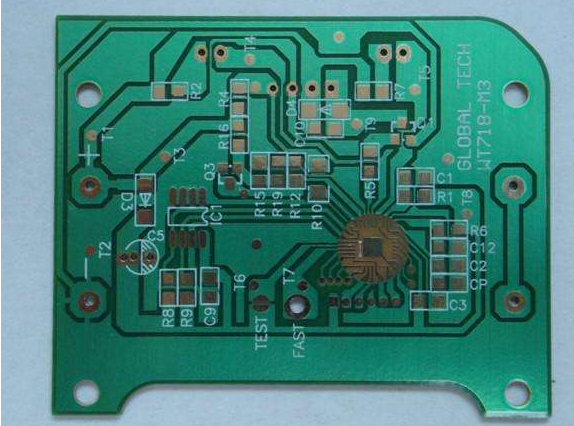
The printed circuit board is composed of copper foil, resin, glass cloth and other materials, and their physical and chemical properties are different. They will inevitably produce thermal stress and cause deformation when pressed together.
At the same time, the PCB board undergoes various processes such as high temperature, mechanical cutting, wet processing, etc., during the processing process, and it will also have an important impact on the deformation of the board. The reasons for the deformation of the PCB board are complex and changeable. How to reduce or Eliminating the deformation caused by different material properties or different processing techniques has become one of the problems for PCB manufacturers.

2.
uses of circuit board deformation.
The deformation of the printed circuit board needs to be studied from several aspects such as material, structure, pattern distribution, processing technology, etc. This article will analyze and explain various reasons and improvement methods that may cause deformation.
The copper spreading area of the plate is uneven, which makes the plate bending and the plate warping worse.
Usually a large amount of copper foil is designed on the circuit board as grounding, and sometimes a large amount of copper foil is also designed on the Vcc layer. When these large amounts of copper foil cannot be evenly distributed on the same circuit board, heat absorption and heat dissipation will occur. The problem of evenness.
Of course, the circuit board is also heat-shrinkable. If the heat-shrinkage cannot cause different stress and deformation at the same time, and the temperature of the board reaches the upper limit of the Tg value, the board will begin to soften and cause deformation.
The junctions (vias, vias) of each layer on the circuit board will limit the lifting of the board.
Modern circuit boards are mostly multi-layer boards. There will be joints between the layers that are the same as the rivets. The joints are divided into through holes, blind holes and buried holes. Where there are joints, the effect of expansion and contraction of the board will be restricted. It will also indirectly cause the board to bend and warp.
Reasons for the deformation of the circuit board:
The weight of the circuit board itself will cause the board to dent and deform.
Usually the reflow furnace adopts a chain structure, which can push the circuit board forward, that is to say, the entire board should be supported on both sides of the board as a fulcrum.
If there are heavy parts on the board, or the size of the board is too large, the phenomenon of depression in the middle will appear due to its own species, which will cause the board to bend.
The depth of the V-Cut and the connecting strip will affect the deformation of the jigsaw.
Fundamentally speaking, V-Cut is the culprit that destroys the structure of the board, because V-Cut is grooved in the original large board, so it is easy to deform at the V-Cut.
The degree of influence of crimping material, structure and graphics on board deformation:
The circuit board is formed by pressing the core board, the prepreg and the outer copper foil. The core board and the copper foil are deformed by heat during the pressing process. The amount of deformation depends on the coefficient of thermal expansion (CTE) of the two materials.
The coefficient of thermal expansion (CTE) of copper is about 17X10-6; the coefficient of thermal expansion (CTE) of FR-4 substrate is about (50~70)X10-6; the coefficient of thermal expansion (250~350) of ordinary FR-4 substrate is and X-direction CTE is generally similar to copper foil due to the presence of glass cloth.
3.
Deformation of the circuit board during processing.
The causes of deformation during circuit board processing are very complex, and can be divided into stresses caused by thermal stress and mechanical stress.
Among these stresses, thermal stress is generated during pressing, and mechanical stress is generated during stacking, handling, and baking of plates. A brief discussion follows in the order of the process.
1. Copper-clad raw materials:
Copper clad laminates are double-layer panels with symmetrical structure and no patterns. The CTE of copper foil and glass cloth are very different, so the deformation caused by the difference in CTE rarely occurs during lamination.
However, due to the large size of the copper clad laminate press and the temperature difference in different areas of the hot plate, there are subtle differences in the curing speed and degree of the resin in different areas during the pressing process. At the same time, the dynamic viscosity varies greatly at different heating rates, so curing will also occur. Local stress during the process.
Under normal circumstances, the stress is kept in balance after pressing, but it is gradually released during subsequent processing, resulting in deformation.
2. Pressing:
The lamination process of printed circuit boards is the main process that generates thermal stress. Similar to the lamination of copper clad laminates, local stresses caused by inconsistencies in the curing process will also occur. The printed circuit boards are thicker and have more patterns, so prepreg It is more difficult to eliminate thermal stress than copper clad laminates.
In addition, the stress on the PCB board will be released during the subsequent drilling, forming or baking process, which will cause the board to deform.
3. Processes such as solder mask and character baking:
Because the solder mask inks cannot be superimposed on each other when they are cured, the circuit boards are all placed on a rack for curing. The solder mask temperature is about 150°C, which just exceeds the Tg point of the Tg material. The resin above the Tg point is highly elastic. The plate is easy to deform under the action of its own weight or the strong wind of the oven.
4. Flatness of hot-air solder:
Generally, the tin furnace temperature of the hot-air soldering machine for plates is between 225°C and 265°C, and the time is 3S-6S. The temperature of the hot air is between 280 and 300 degrees Celsius.
At room temperature, the solder is transferred from room temperature to the tin furnace, and then the post-treatment water washing at room temperature is carried out within two minutes after being out of the furnace. The whole process of hot air solder leveling is a rapid cooling process.
Because the material of the circuit board is different, its structure is not uniform, it will inevitably produce thermal stress during the cooling and heating process, resulting in microscopic strain and overall deformation warping zone.
5. Storage:
Printed circuit boards are stored in the semi-finished product stage, and they are usually hard inserted on the shelf. Improper adjustment of the shelf tightness, or stacking or placing the board during the storage process will cause mechanical deformation of the board. In particular, it has a greater impact on plates below 2.0mm.
In addition to the above factors, there are many factors that affect the deformation of the PCB board.
4.
Prevent warping and deformation of the circuit board.
The warping deformation of PCB circuit board has a great influence on the production of printed circuit board. Warpage deformation is also an important problem in circuit board production. The board with components will bend after soldering, which makes it difficult for the component feet to be neat. .
The board cannot be installed on the chassis or socket, therefore, the warpage of the circuit board will affect the normal operation of the entire subsequent process.