1. What are the special features of PCB copying skills?
As we all know, one of the necessary skills of PCB copy board electronic engineer is circuit design, which shows the importance of circuit design. The related content of circuit design mainly includes two aspects: circuit schematic design and printed circuit board design. Generally speaking, there is a small shortcut to learning circuit design, which is to analyze classic designs. Classical design also has many applications. For example, mass production of electronic products is one of them, as well as displays.
The analysis of a classic design generally has the following steps, which generally include tablet readings, reverse push schematics, simulation analysis (which can be excluded) and modify the design to suit your application. Among them, plate reading is a kind of learning, the first step is also a relatively important step. Board reading is a PCB board design that uses reverse technology for research.
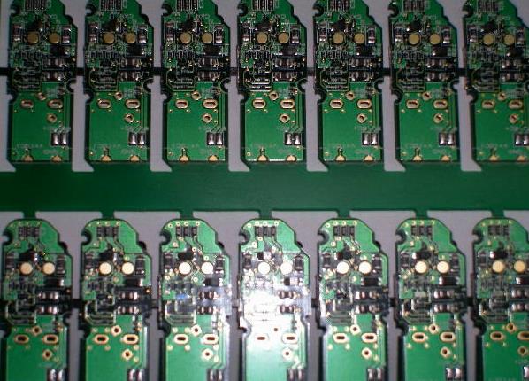
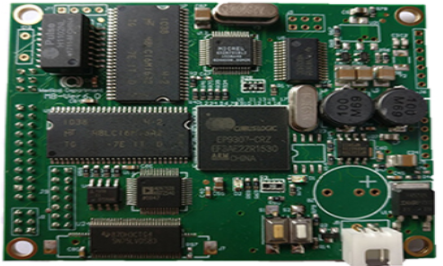
First of all, we introduce to you the method of PCB copying and the steps to be performed. PCB copy board can also be said to be clone, which belongs to the reverse engineering part of PCB design. This requires removing all the components on the PCB circuit board, and then scanning the empty board into a picture, and recovering it to the PCB board drawing file through the board software processing.

Any electronic product can be imitated or electronic through PCB copying and reverse technology. Product clone. In the inventory production process, first we need to clearly mark the content and data related requirements. In fact, in the making of the list, seemingly simple things hide a lot of learning. First of all, we should make corresponding preparations. First get a PCB, and use a better camera to photograph the positions of the two gases. The effect of the photograph must be clear, otherwise it is impossible. Then we need to write down a series of models, parameters and positions on the paper, especially the diode, the direction of the three tubes and so on. Be sure to remember. The next step is to publish the record. Let's delete all devices from the beginning. It should be noted that we know the number of related equipment and parameters, each component is deleted, corresponding to its position number and double-sided tape, etc. pasted on the white paper.
Remind you that in the process of splitting the board, you must be especially careful about the number of components arranged for each person, because a small detail may lead to the cancellation of the entire project and affect the effect of the final clone. The last step is component testing. First of all, we get the relevant data list from the disassembly personnel, and we can formally enter the BOM production process, that is, through various tests and analyses, all the components of the relevant parameters are converted into the system table process. This is when we need to use an advanced instrument called Bridge Tester. The tester is mainly used for impedance analysis of various components of the measuring instrument. It uses advanced comparison methods to measure the resistance, capacitance and inductance of the components.
Of course, different levels of bridge test equipment have different test results and accuracy. Generally speaking, the bridge tester is divided into many types according to different grades. The use of this instrument can not only ensure higher accuracy, but also improve the intensity and efficiency of the measurement. Therefore, the PCB circuit board is more complicated and requires certain skills.
Second, the characteristics of the circuit board micro-hole mechanical drilling
Now that electronic products are renewing rapidly, PCB printing has expanded from the previous single-layer boards to double-layer boards and multi-layer boards with more complicated high-precision requirements. Therefore, there are more and more requirements for the processing of circuit board holes, for example, the hole diameter is getting smaller and smaller, and the distance between the holes is getting smaller and smaller. It is understood that epoxy resin-based composite materials are more commonly used in board factories. The definition of hole size is that the diameter of 0.6mm or less is a small hole, and the diameter of less than 0.3mm is a micro hole.
Today I will introduce the processing method of micro-holes: mechanical drilling. In order to ensure higher processing efficiency and hole quality, we reduce the proportion of defective products. In the process of mechanical drilling, two factors, axial force and cutting torque, must be considered, which may directly or indirectly affect the quality of the hole. The axial force and torque will increase with the feed rate and the thickness of the cutting layer, so the cutting speed will increase, so that the number of cut fibers per unit time will increase, and the amount of tool wear will also increase rapidly.
Therefore, the life of the drill is different for holes of different sizes. The operator should be familiar with the performance of the equipment and replace the drill in time. This is also the reason why the processing cost of micro holes is higher. The static component force FS of the axial force affects the cutting of the chisel edge, while the dynamic component force FD mainly affects the cutting of the main cutting edge. The dynamic component force FD has a greater impact on the surface roughness than the static component force FS. Generally, when the diameter of the prefabricated hole is less than 0.4mm, the static component force FS decreases sharply with the increase of the diameter, while the dynamic component force FD decreases more flatly.
The wear of the PCB drill bit is related to the cutting speed, feed rate, and the size of the slot. The ratio of the drill radius to the glass fiber width has a greater impact on the tool life. The larger the ratio, the larger the width of the tool cutting fiber bundle, and the increase in tool wear. In practical applications, a drill life of 0.3mm can drill 3000 holes. The larger the drill, the fewer holes to drill.
In order to prevent problems such as delamination, hole wall damage, stains, and burrs during drilling, we can first put a 2.5mm thickness backing board underneath during the delamination, put the copper clad laminate on the backing board, and then Put an aluminum sheet on the copper clad laminate. The function of the aluminum sheet is:
1: Protect the board surface from scratching.
2: Good heat dissipation, the bit will generate heat when drilling.
3: Buffering/drilling function to prevent partial holes. The method to reduce burrs is to use vibration drilling technology, using carbide drills to drill, the hardness is good, the size and structure of the tool also need to be adjusted.