1. What should be paid attention to for moisture-proof insulation of PCB circuit boards?
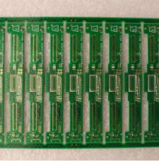
The circuit board can be called a printed circuit board or a printed circuit board, the English name is "Printed Circuit Board" PCB, (flexible printed circuit board) FPC circuit board (FPC circuit board, also known as flexible circuit board flexible circuit board) Highly reliable and excellent flexible printed circuit boards made of imide or polyester film substrates have high wiring density, light weight, thin thickness, good bending characteristics, and flexible and rigid boards (reechas, soft Hard board) The development of FPC and PCB has given birth to new products of hard board and soft board.
The circuit board needs to be moisture-proof and insulated during the assembly and use of electronic equipment, so it is bound to become the moisture-proof insulating UV glue for electronic circuit boards.
The use process of the special moisture-proof insulating UV glue for electronic PCB:
Best operation: apply glue or brush directly, if the concentration becomes larger, you can also add a thinner.
Spraying process:
1: CRCBOND UV773 can be diluted with a special thinner, the amount of thinner added is large, the viscosity of the adhesive is low, and the thickness of the glue is thin;
2: Put the diluted glue in a spray pot and spray it.
3: Clean the spray pot with thinner after spraying.
Soaking process:

1: Same as 1.1
2: Immerse the diluted glue into the soaking bucket. When used for soaking, the soaking speed of the circuit board or components should not be too fast to avoid air bubbles. The drying time of a normal thermometer is 2-10 minutes, heating and drying are not recommended.
3: When you use it again after the immersion coating is over, if there is a hard skin on the surface, please remove the skin and continue using it.
2. PCB design via and copper connection
In PCB design, design rules design rules are the key to the success or failure of PCB design. The intention of all PCB designers is to drive and realize the functional manifestation of PCB design through the soul of PCB design rules. Exquisite and detailed rule definitions can help designers in the PCB layout and routing work, save a lot of engineers a lot of energy and time, help PCB designers to achieve excellent PCB design, greatly facilitating PCB design work.
The entire PCB design needs to comply with the rule definition. Including the most basic electrical rules (spacing, short-circuit interruption), PCB wiring rules (line width, line type, through-hole style, fan-out, etc.), plane rules (power floor layer connection, copper connection method) and other commonly used auxiliary rules, Such as layout rules, manufacturing rules, high-speed PCB design rules, signal integrity rules, etc. After completing the PCB design, you can also check the PCB design through the rule check design rules to see if there is a rule violation and improve it.
Rule-based techniques for PCB copper design. Describes how to change the connection method of the copper cable and the through hole in altium Designer when designing the copper cable, and reduce the edge of the circuit board.
The cross-sectional shape of the cross-holes should be such that the perforated connections on the copper-clad PCB board do not cross but directly cross, and the "plane-polygon" connection style can be set in the "design rules". The default setting above is to release the connection, which is a cross-flower connection like a thermal pad. Add a rule and set the object to all through Svia in the Query statement. The rule is set to direct connection. After re-laying the copper wire. The connection of the cross-shaped flower is eliminated.
In the PCB design and manufacturing industry, generally speaking, due to the mechanical considerations of the finished circuit board, or to prevent the copper skin from being exposed to the edge of the board, which may cause roller edges or electrical short circuits, engineers often spread large areas of copper relative to The block at the edge of the board shrinks to 20 mils instead of all the way to the edge of the board. There are many ways to treat this copper skin depression. For example, draw a reserved layer on the edge of the circuit board, and then set the distance between the copper and the reserved layer. A simple method is to set different safety distances for copper paving objects. For example, the safety distance for the entire board is set to 10 mils, and the safety distance for copper paving is 20 mils. The effect of reducing the edge of the board by 20 mils can be achieved. It can also remove dead copper that may appear in the device. There are many ways to reduce the inner edge of the circuit board. These methods use Query statements to be more accurate and more convenient to accurately set copper objects.