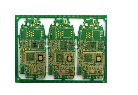
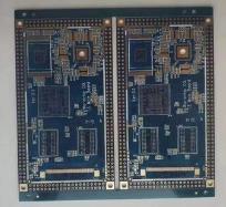
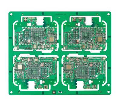
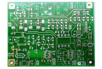
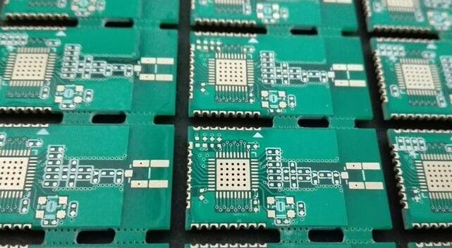
PCB production: process flow of multilayer PCB1
1. What is the purpose of blackening and browning when Shenzhen PCB Factory produces multilayer PCBs?
1. Remove oil, impurities and other pollutants on the surface;
2. The oxidized surface is not affected by moisture at high temperatures, reducing the chance of delamination between the copper foil and the resin;
3. Make the non-polar copper surface into a surface with polar CuO and Cu 2 O, and increase the polar bond between the copper foil and the resin;
4. increase the specific surface of the copper foil, thereby increasing the contact area with the resin, which is conducive to the full diffusion of the resin and the formation of a greater bonding force;
5. The board with the inner circuit must be blackened or browned before it can be laminated. It is the circuit copper meter for the inner board
The surface is oxidized. Generally, Cu 2O is red and CuO is black, so Cu 2O in the oxide layer is mainly called browning, and CuO-based is called blackening.
1. Laminating is the process of bonding each layer of circuits into a whole by means of a B-stage prepreg. This bonding is achieved through the mutual diffusion and penetration of macromolecules at the interface, and then interweaving. The stage prepreg is the process of bonding each layer of circuits into a whole. This bonding is achieved through the mutual diffusion and penetration of macromolecules at the interface, and then interweaving.
2. Purpose: to press discrete multi-layer PCB boards together with adhesive sheets into multi-layer boards with the required number of layers and thickness.

1. The laminated circuit board is sent to the vacuum heat press during the lamination process. The heat energy provided by the machine is used to melt the resin in the resin sheet, thereby bonding the substrate and filling the gap.
2. The typesetting combines copper foil, bonding sheet (prepreg), inner layer board, stainless steel, isolation board, kraft paper, outer layer steel plate and other materials according to the process requirements. If there are more than six layers of circuit boards, pre-composition is required.
3. Lamination For designers, the first thing that needs to be considered for lamination is symmetry. Because the board will be affected by pressure and temperature during the lamination process, there will still be stress in the board after the lamination is completed. Therefore, if the two sides of the laminated board are not uniform, the stress on the two sides will be different, causing the board to bend to one side, which greatly affects the performance of the PCB.
In addition, even in the same plane, if the distribution of copper is uneven, the resin flow speed at each point will be different, so that the thickness of the place with less copper will be slightly thinner, and the thickness of the place with more copper will be thicker. Some. In order to avoid these problems, various factors such as the uniformity of copper distribution, the symmetry of the stack, the design and layout of blind and buried vias, etc. must be carefully considered during the design.
2. Decontamination and copper sinking
1. Purpose: Metallize the through hole.
1. The base material of circuit board proofing is composed of copper foil, glass fiber, and epoxy resin. In the production process, the hole wall section after the base material is drilled is composed of the above three parts of materials.
2. Hole metallization is to solve the problem of covering a uniform layer of copper with heat shock resistance on the cross section. Hole metallization is to solve the problem of covering a uniform layer of copper with heat shock resistance on the cross section.
3. The process is divided into three parts: one is the de-drilling process, the second is the electroless copper process, and the third is the thickening process (copper plating on the whole board).