Step: process design
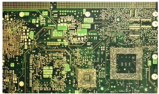
The process of surface adhesion assembly, especially for small spacing components, needs continuous monitoring and systematic inspection. For example, in the United States, the solder joint quality standard is based on ipc-a-620 and national solder standard ANSI / j-std-001. Only by understanding these criteria and specifications can designers develop products that meet the requirements of industrial standards.
Mass production design
Mass production design includes the process, assembly, testability and reliability of all mass production, and is based on written document requirements.
A complete and clear assembly document is absolutely necessary and successful for a series of transformations from design to manufacturing. The relevant documents and CAD data list include bill of materials (BOM), list of qualified manufacturers, assembly details, special assembly guidelines, PC board manufacturing details and Gerber data or ipc-d-350 program contained in the magnetic disc.
The CAD data on the magnetic disc is very helpful to develop test and process tools, and to program automatic assembly equipment. It includes X-Y axis coordinate position, test requirement, outline graph, circuit diagram and X-Y coordinate of test point.

PCBA quality
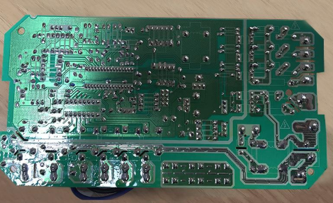
Take a sample from each batch or a specific batch number to test its solderability. The PCBA will be compared with the product information provided by the manufacturer and the quality specification calibrated on IPC. The next step is to print the solder paste onto the pad and solder back. If organic flux is used, it needs to be cleaned again to remove the residue. When evaluating the quality of solder joint, we should also evaluate the appearance and size reaction of PCBA after reflow. The same test method can also be used in the wave soldering process.
Assembly process development
This step includes the continuous monitoring of each mechanical action with the naked eye and automatic visual devices. For example, it is recommended to use laser to scan the paste volume printed on each PC board.
After the sample is put on the SMD and soldered back, the quality control and engineering personnel need to check the tin eating status of each component connector one by one. Each member needs to record the alignment of passive components and multi pin components in detail. After the wave soldering process, it is also necessary to carefully inspect the uniformity of solder joints and to determine the potential locations of defects in solder joints due to the proximity of the pins or components.
Fine pitch technology
Fine pitch assembly is an advanced construction and manufacturing concept. The density and complexity of the components are much higher than the mainstream products in the current market. If we want to enter the mass production stage, we must modify some parameters before putting them into the production line.
For example, the pin pitch of the fine pitch element is 0.025 "or less, which can be applied to standard and ASIC components. For these components, the industry standard has a very wide allowable error, as shown in Figure 1. It is because the tolerance errors of component suppliers are different from each other, so the pad size must be customized or modified to improve the assembly yield.
The dimension and spacing of pad are generally in accordance with ipc-sm-782a. However, in order to meet the requirements of the process, the shape and size of some pad will be slightly different from this specification. For wave soldering, the pad size is usually a little larger in order to have more flux and solder. It is necessary to adjust the pad size properly for some components which are usually kept near the upper and lower limits of process tolerance.
Consistency of placement orientation of surface adhesive components
Although it is not necessary to design all components in the same orientation, consistency will help to improve assembly and inspection efficiency for the same type of components. For a complex board, components with pins usually have the same orientation to save time. The reason is that the gripper for placing components is usually fixed in one direction, and the placement orientation can only be changed by rotating the board. As for the general surface adhesive components, there is no such problem because the gripper of the placement machine can rotate freely. However, in order to pass the wave soldering furnace, it is necessary to unify the orientation of components to reduce the exposure time of tin flow.
The polarity of some components with polarity has been determined as early as the whole circuit design. After understanding the circuit function, the process engineer can decide the order of placing components to improve the assembly efficiency, but the efficiency can be improved by having the same directivity or similar components. If the placement orientation can be unified, not only the speed of writing placement component program can be shortened, but also the occurrence of errors can be reduced.
Consistent (and adequate) component distance
Generally speaking, the full-automatic surface adhesive placement machine is quite accurate. However, designers often ignore the complexity of mass production while trying to increase the density of components. For example, when a high component is too close to a component with a small pin pitch, it will not only block the line of sight for inspection of the pin solder joint, but also hinder the tools used for rework or rework.
Wave soldering tin is generally used in low and short components such as diodes and transistors. Small components such as SOIC can also be used on wave soldering tin, but it should be noted that some components cannot withstand the high heat directly exposed to the tin furnace.
In order to ensure the consistency of assembly quality, the distance between components must be large enough and evenly exposed to the tin furnace. In order to ensure that the solder can contact each contact, the high component should keep a certain distance from the low and low components to avoid shielding effect. If the distance is not enough, it will also hinder the inspection and rework of components.
Industry has developed a set of standard applications for surface adhesive components. If possible, standard components should be used as much as possible, so that designers can establish a database of standard pad sizes and engineers can better grasp the process problems. Designers can find that some countries have established similar standards, and the appearance of components may be similar, but the pin angle of components varies from country to country. For example, the suppliers of SOIC components from North America and Europe can meet the Eiz standard, while the Japanese products take EIAJ as the design criterion. It should be noted that even if they meet the EIAJ standard, the components produced by different companies are not identical in appearance.
Designed to improve productivity
The assembly board can be quite simple or very complex, depending on the shape and density of the components. A complex design can make efficient production and reduce the difficulty, but if the designer does not pay attention to the process details, it will become very difficult. The assembly plan must be considered at the beginning of the design. Generally, as long as the position and orientation of the components are adjusted, the mass production can be increased. If the size of a PC board is very small, with irregular shape or components close to the edge of the board, mass production can be considered in the form of connecting plates.
Testing and repair
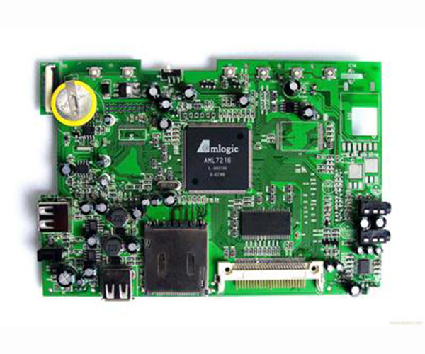
It is very inaccurate and time-consuming to use small-scale test tools on the table to detect missing components or process. The test method must be considered in the design. For example, if you want to use ICT testing, you should consider designing some test points on the line that the probe can contact. There is a program written in advance in the test system, which can test the function of each component, point out which component is faulty or misplaced, and judge whether the solder joint is in good condition. The detection error should also include the short circuit between the component contacts and the empty welding between the pin and the pad.
If the test probe cannot touch each common junction on the line, it is impossible to measure each component individually. Especially for the assembly of micro pitch, the probe of automatic test equipment is needed to measure the connected points on all lines or the lines connected between components. If you can't do this, you have to pass the function test if you can't, otherwise you have to wait for the customer to wear out after shipment.
ICT testing is to make different tools and test procedures according to different products. If testing is considered in the design, the quality of each component and contact can be easily detected. (Fig. 2) the solder joint defect can be seen visually. However, tin deficiency and very small short circuits are only checked by electrical tests.
Since the density of the components on the surface and the second side may be identical, the traditional test method may not be able to detect all errors. Although there is a small via pad on the PC board with high density and fine pitch for the probe to contact, it is still desirable to increase the via pad for use.