One: line
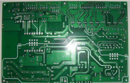
Minimum line width: 6mil (0.153mm). In other words, if the line width less than 6 million cannot be produced, if the design conditions allow, the larger the line width is, the better, the larger the line width, the better the PCB factory production, the higher the yield, the general design routine is about 1,000 If this is very important, the design must be considered
Minimum line length: 6mil (0.153mm). The minimum line spacing is the line spacing line and the distance between the line and the pad. From a production point of view, it is not less than 6 mils. The larger the better, it is generally within 10 mils. Of course, it is the design condition. The larger the better, this is very important. Design must be considered
The line spacing of the line pair table is 0.508mm (20mil)
Two: through holes (usually called conductive holes)
Minimum aperture: 0.3 mm (12 million)

The minimum via hole (VIA) aperture is not less than 0.3mm (12mil), and the single-side pad cannot be less than 6mil (0.153mm), preferably greater than 8mil (0.2mm). The maximum limit (see Figure 3) is important, the design must be considered
The hole spacing (hole edge to hole edge) of each via hole (VIA) cannot be less than: 6mil is preferably greater than 8mil. This is very important and must be considered in the design
The distance between the PCB pad and the molding line is 0.508mm (20mil)
Hole spacing:
NPTH (no welding ring): hole compensation is 0.15MM, the back line is above 0.2MM
PTH (with welding ring): hole repair 0.15MM back distance line more than 0.3MM
Hole spacing:
PTH (with welding ring): hole to hole above 0.45MM, rear hole compensation 0.15MM
NPTH hole: after 0.2MM or higher between the hole and the hole, the hole compensation is 0.15MM
VIA: Slightly spaced
Three: PAD PAD (usually called insertion hole (PTH))
The size of the insertion hole depends on your component, but it must be larger than your component pin. It is recommended to be at least 0.2mm or larger, that is, 0.6 component pin. You must design at least 0.8. In order to prevent processing tolerances from making it difficult to insert,
The single side of the outer ring of the insertion hole (PTH) pad cannot be less than 0.2mm (8mil), of course, the larger the better (as shown in Figure 2 solder entry). This is very important and must be considered in the design
The hole distance (hole edge to hole edge) of the plug-in hole (PTH) cannot be less than: 0.3mm, of course, the larger the better (as shown in Figure 3), this is very important, and the design must be considered
The distance from the pad to the table is 0.508mm (20mil)
Other considerations.
The shape of the PCB board (such as the board frame, slot, V-CUT) must be placed in the KEEPOUT layer or the mechanical layer, and cannot be placed in other layers, such as the silk screen layer and the wire layer. All grooves or holes that need to be mechanically formed should be placed on one layer as much as possible to avoid leakage or holes.
If the shape of the PCB mechanical layer and the KEEPOUT layer are inconsistent, please specify that in addition to the shape to be given effective shape, if there is an inner groove, and the outer shape of the inner groove intersects, the outer shape of the sector to be removed will be affected by the mechanical The mechanical layer of the grooves and holes of the KEEP OUT layer and the mechanical layer of the KEEP OUT layer and the non-leakage gongs designed in the KEEP OUT layer are usually made according to the copper-free PCB (the copper should be removed when making the Filin). The metal holes need to be processed, please Special Note.
If you want to make a metalized slot hole, the most reliable method is to put multiple pads together, then this approach will not go wrong
Please pay special attention to whether you need to do diagonal chamfering when ordering golden finger boards.
For GERBER files, please check whether there is a small layer phenomenon in the files, usually our department will directly produce according to THE GERBER files.