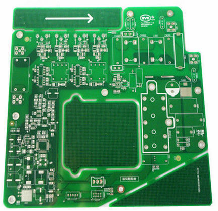
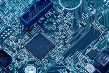
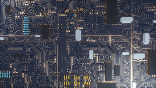
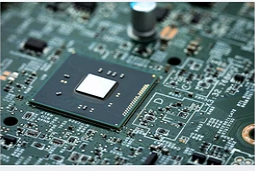
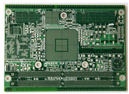
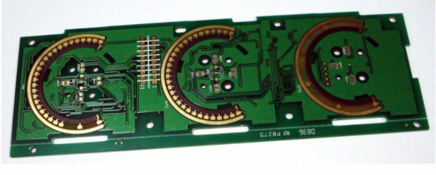
PCB circuit board copper reasons and PCB circuit board substrate classification
In the process of PCB proofing, some process defects are often encountered, such as poorly falling off of the copper wire of the PCB circuit board (also often referred to as copper shaking), which affects the quality of the product. The common reasons for the PCB circuit board copper are as follows: First, the process factors of the PCB circuit board:
1: Copper foil is etched too much. Electrolytic copper foil used in the market is generally used for single-sided galvanizing (commonly known as gray foil) and single-sided copper plating (commonly known as red foil). Ordinary polished copper generally exceeds that of bulk copper. 70um galvanized copper foil, red foil and 18um gray foil.
2: PCB process local collision, the copper wire is separated from the substrate by external force. This poor performance is poor positioning or directionality, and the dropped copper wire will be significantly deformed or deformed in the same direction as the scratch/impact mark. The copper wire peeled off badly. Looking at the copper foil, you can see that the color of the copper foil hair surface is normal, there will be no bad side corrosion, and the copper foil peeling strength is normal.

3: The PCB circuit board design is unreasonable, and the thick copper foil design line is too thin, which will also cause the circuit to be over-etched and shake the copper wire.
Reasons for laminate processing:
Under normal circumstances, as long as the high temperature section of the hot pressing exceeds 30 minutes, the copper foil and the prepreg can basically be completely combined, so the joint connection generally does not affect the bonding force of the laminated copper foil and the substrate. However, during the laminate stacking process, if PP pollution or copper foil damage, it will also cause the combination of copper foil and substrate after the laminate is insufficient, which will result in positioning (only for large boards) or sporadic copper wire falling off, but the test There is no abnormality in the peel strength of the copper foil near the wire.
Reasons for laminate raw materials:
1: Ordinary electrolytic copper foils are all coated or copper-plated products. If the peak period of wool foil production is abnormal, or galvanized/coppered, the coating branch is not good enough, resulting in the peeling strength of the copper foil itself Not enough. After inserting the plug-in in the electronics factory, the defective foil press board is made into a PCB, and the copper wire will be impacted by the external force and fall off. This kind of bad copper stripped copper wire that looks at the rough surface of the copper foil (that is, in contact with the substrate) will not produce obvious corrosion, but the peeling strength of the entire copper foil will be very poor.
2: The adaptability of copper foil and resin is not good: now use some special performance laminates, such as HTg board, because the resin system is different, the curing agent used is generally PN resin, the resin molecular chain structure is simple, low cross-linking When curing, it is bound to match it with a special peak copper foil. When the copper foil and resin system used in the laminated board produced do not match, the peeling strength of the coated metal foil is insufficient, and the plug-in will also have the problem of copper wire falling off.
As the name implies, the substrate is the basic material for manufacturing PCB circuit boards. The general PCB substrate is composed of resin, reinforcing materials, and conductive materials, and there are many types. The resin is the more common epoxy resin, phenolic resin, etc. The reinforcing material includes paper base, glass cloth, etc. The most commonly used conductive material is copper foil. Copper foil is divided into electrolytic copper foil and embossed copper foil.
PCB substrate material classification:
First of all, according to the different techniques of reinforcing materials:
1: Paper substrate (FR-1, FR-2, FR-3).
2: Epoxy glass fiber cloth substrate (FR-4, FR-5).
3: Composite substrate (CEM-1, CEM-3 (composite epoxy material grade 3).
4: HDI (High Density Interconnection Network High Density Interconnection) table (RCC).
Special substrates (metal substrates, ceramic substrates, thermoplastic substrates, etc.).
According to flame retardant performance:
1: Flame-retardant type (UL94-V0, UL94V1).
2: Non-flame retardant (UL94-HB grade).
According to different resins:
1: Phenolic resin board.
2: Epoxy board.
3: Polyester resin board.
4: BT resin board.
5: PI resin board.