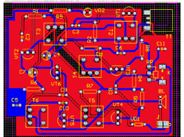
1, What is copper clad PCB
The so-called PCB copper coating is to take the idle space on the PCB as the reference plane, and then fill the PCB with solid copper. These copper areas are also called copper filling.
The significance of copper clad PCB lies in: reducing ground impedance, improving anti-interference ability; reducing voltage drop, improving power efficiency; connecting with ground wire, can also reduce loop area.
For the purpose of keeping the PCB from deformation as much as possible, most PCB manufacturers also require the PCB designer to fill the open area of PCB with copper sheet or grid like ground wire. If the PCB copper coating is handled improperly, it will not be worth the loss. Is the PCB copper coating "advantages greater than disadvantages" or "disadvantages greater than advantages"? We all know that in the case of PCB high frequency, the distributed capacitance of wiring on the printed circuit board (PCB) will work. When the length is greater than 1 / 20 of the corresponding wavelength of the noise frequency, antenna effect will occur, and the noise will be emitted through the wiring. If there is poor grounding of PCB copper coating in the PCB, PCB copper coating will become a tool for noise transmission.

PCB solid copper
Therefore, in the high-frequency PCB circuit, do not think that a certain place of the ground wire is grounded, which is the "ground wire". Holes must be drilled in the wiring with a spacing less than λ / 20, so as to be "well grounded" with the ground plane of the multilayer board. If the proper treatment of PCB copper coating, PCB copper coating not only increases the current, but also plays a dual role in shielding interference.
2, Two forms of copper clad PCB
There are two basic ways of PCB copper coating, that is, large area PCB copper coating and PCB grid copper coating. It is often asked whether large area PCB copper coating is better or PCB grid copper coating, which is not easy to generalize.
Why? Large area PCB copper coating has the dual functions of increasing current and shielding. However, if the large area PCB is covered with copper, the board may be warped and even blistered when soldering. Therefore, a large area of PCB copper, will generally open a few slots to ease the blistering of copper foil.

PCB grid copper
Pure PCB grid copper coating is mainly for shielding, and the effect of increasing current is reduced. From the perspective of heat dissipation, grid is beneficial (it reduces the copper heating surface) and plays a certain role in electromagnetic shielding. Especially for the touch circuit, as shown in the following figure: it should be pointed out that the grid is composed of lines in staggered directions. We know that for PCB circuits, the width of the line has its corresponding "electrical length" for the working frequency of PCB (the actual size can be obtained by dividing the digital frequency corresponding to the working frequency, see relevant books for details).
When the working frequency is not very high, perhaps the role of PCB gridlines is not very obvious. Once the electrical length and working frequency match, it will be very bad. You will find that the PCB circuit can not work normally at all, and the signals interfering with the system are being transmitted everywhere.
The suggestion is to choose according to the working condition of the PCB designed. Don't hold on to something. Therefore, high frequency PCB circuit requires high multi-purpose grid to resist interference, low-frequency PCB circuit with high current circuit and other commonly used complete PCB copper.