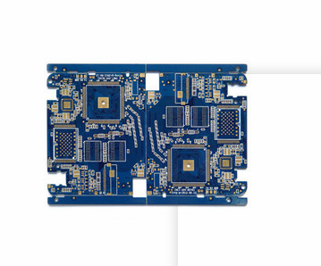
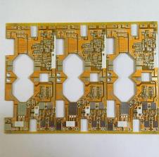
One, the detection method of assembling PCB multilayer circuit board
In order to meet the requirements of PCB multi-layer circuit board testing, various test equipment came into being. The automatic optical inspection (AOI) system is usually used to inspect the inner layer before delamination; after delamination, the X-ray system monitors the alignment accuracy and small defects; the scanning laser system provides a way to inspect the pad layer before reflow soldering. method. The combination of these systems with the visual inspection technology of the production line and the component integrity inspection technology of automatic component placement helps to ensure the reliability of the final assembly and welding of the panels.
However, even with these efforts to minimize defects, it is still necessary to perform final inspection on the assembled PCB multilayer circuit board, which may be the most important because it is the final unit of product and overall process evaluation.
The final inspection of the assembled PCB multi-layer circuit board can be done with a dynamic method or an automatic system, and these two methods are often used together. "Manual" means that the operator visually inspects the board with optical instruments and makes correct judgments on defects. The automated system uses computer-aided graphical analysis to determine defects. Many people also believe that automated systems include all detection methods except artificial light detection.

X-ray technology provides a method for evaluating solder thickness, distribution, internal voids, cracks, desoldering, and the presence of solder balls (Markstein, 1993). Ultrasound can detect voids, cracks and unbonded interfaces. Automatic optical inspection evaluates external features such as bridging, flux and shape. Laser inspection can provide three-dimensional images of external features. Infrared detection compares the thermal signal of the solder joint with a known good solder joint to detect internal faults in the solder joint.
It is worth noting that all the defects that cannot be found by the limitation of the automatic inspection technology of the assembled PCB multilayer circuit board have been found. Therefore, artificial visual inspection methods must be combined with automatic inspection methods, especially for those applications that are less frequently used. The combination of X-ray inspection and manual optical inspection is the best method to detect defects in the assembly board.
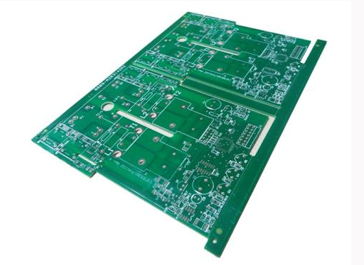
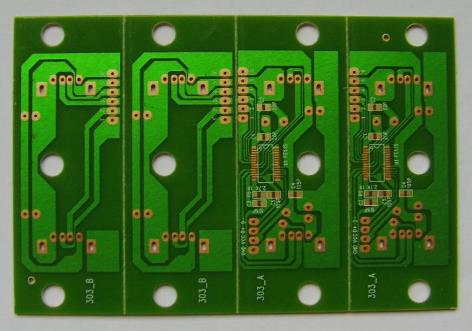
Assembled and soldered PCB multilayer circuit boards are prone to the following defects:
1) Missing parts;
2) Component failure;
3) There are installation errors and misplaced components;
4) Component failure;
5) Poor tin staining;
6) Bridge
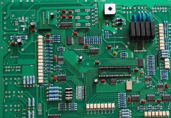
2. SMT processing surface assembly process inspection
The quality and reliability of surface mount products mainly depend on the manufacturability and reliability of components, electronic process materials, process design and assembly processes. In order to successfully assemble SMT products, on the one hand, the quality of electronic components and process materials must be strictly controlled, that is, incoming inspection; on the other hand, the manufacturability (DFM) audit of SMT process design must be conducted for the assembly process. During the implementation of the assembly process, process quality inspection must be carried out before and after each process, that is, surface assembly process inspection, including the quality inspection methods and strategies of each process in the entire assembly process such as printing, installation, and welding.
1) Test content of solder paste printing process
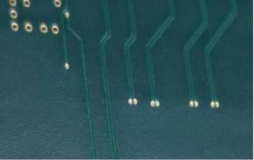
Solder paste printing is the starting point of the SMT process, and it is the most complex and unstable process. It is affected by many factors and has dynamic changes. It is also the source of most defects. 60%-70% of defects appear in the printing stage. If an inspection station is set up after printing to detect the quality of solder paste printing in real time and eliminate defects in the initial stage of the production line, losses and costs can be minimized. Therefore, more and more SMT production lines are equipped with automatic optical inspection for printing, and even some printing machines are also integrated with AOI and other solder paste printing inspection systems. Common printing defects in the solder paste printing process include no solder pads, excessive solder, solder paste scratching in the middle of a large pad, solder paste sticking to the edge of a small pad, printing offset, bridging and smearing. Improper processing of template thickness and hole wall, unreasonable printer parameter settings, insufficient precision, improper selection of squeegee material and hardness, poor PCB processing, etc.
2) The content of the component installation process test
The placement process is one of the key processes of the placement production line. It is one of the key factors that determine the degree of automation, assembly accuracy and productivity of the assembly system. It has a decisive impact on the quality of electronic products. Therefore, real-time monitoring of the placement process is of great significance to improve the quality of the entire product. The flow chart of pre-furnace (post-placement) inspection is shown in Figure 6-3. The most basic method is to configure AOI after the high-speed placement machine and before reflow soldering to check the quality of the chip. On the one hand, it can prevent defective solder paste printing and chips from entering the reflow soldering stage, which will cause more trouble; on the other hand, it can provide support for timely proofreading and maintenance of the placement machine, so that the placement machine is always in good condition. The operating status of the. The inspection content of the placement process mainly includes the placement accuracy of components, the placement control of small-pitch devices and BGA, various defects before reflow, such as missing and deviation of components, collapse and deviation of solder paste, etc., PCB surface contamination, There is no contact between the pins and the solder paste. Use character recognition software to read the component value and polarity recognition to determine whether the pasting is wrong.
3) Welding process inspection content
After the welding inspection, a 100% full inspection of the product is required. Usually need to check the following: whether the surface of the solder joint is smooth, whether there are holes, holes, etc.; check whether the shape of the solder joint is half moon, whether there is more or less tin; check whether there are monuments, bridges, element displacement, element missing, tin Beads and other defects; check the polarity defects of all components; check for short circuits, open circuits and other defects in soldering; check the color changes on the PCB surface.