One refers to the processing technology of the production of printed circuit boards;
The second refers to the assembly process of the circuit and structural components and the printed circuit board.
Regarding the processing technology of the production of printed circuit boards, general PCB manufacturers, due to their manufacturing capabilities, will provide designers with relevant requirements in great detail, which is relatively better in practice.
According to the author's understanding, the second category is the manufacturability design for electronic assembly.
The focus of the article is also to describe the manufacturability issues that designers must consider at the stage of PCB design.
1. Appropriate choice of assembly method and component layout
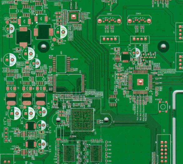
The choice of assembly method and component layout is a very important aspect of PCB manufacturability, which has a great impact on assembly efficiency, cost, and product quality. In fact, the author has been exposed to quite a lot of PCBs and considered some very basic principles. There are also shortcomings.
Choose the right assembly method
Generally, according to the different assembly density of PCB, the recommended assembly methods are as follows:
What is the manufacturability of PCB design
As a circuit design engineer, you should have a correct understanding of the PCB assembly process flow you are designing, so that you can avoid making some principled mistakes. When choosing an assembly method, in addition to considering the assembly density of the PCB and the difficulty of wiring, it must also be based on the typical process flow of this assembly method and the level of the company's own process equipment.
If the company does not have a better wave soldering process, then choosing the fifth assembly method in the above table may bring yourself a lot of trouble.
Another point worth noting is that if you plan to implement a wave soldering process on the soldering surface, you should avoid arranging a few SMDs on the soldering surface to make the process complicated.
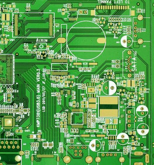
PCB layout of components

The layout of the components on the PCB has a very important impact on production efficiency and cost, and is an important indicator to measure the installability of the PCB design.
Generally speaking, the components are arranged as evenly, regularly and neatly as possible, and arranged in the same direction and polarity distribution.
The regular arrangement is convenient for inspection, is helpful to increase the patch/plug-in speed, and the uniform distribution is beneficial to the optimization of heat dissipation and welding process.
On the other hand, in order to simplify the process, PCB designers must always know that on any side of the PCB, only a group soldering process of reflow soldering and wave soldering can be used.
This is especially worth noting when the assembly density is high and the soldering surface of the PCB must be distributed with more SMD components.
The designer should consider which group soldering process to use for the mounted components on the soldering surface. The most preferred is to use the wave soldering process after the patch is cured, which can simultaneously solder the pins of the perforated device on the component surface; but the wave There are relatively strict constraints on soldering SMD components, and only chip resistors and capacitors of 0603 and above size, SOT, SOIC (pin spacing ≥ 1mm and height less than 2.0mm) can be soldered.
For components distributed on the soldering surface, the pin direction should be perpendicular to the PCB transmission direction during wave soldering to ensure that the solder ends or leads on both sides of the component are dip-soldered at the same time. The arrangement order and spacing between adjacent components should also meet The requirement of wave soldering to avoid "shading effect", as shown in Figure 1. When wave soldering SOIC and other multi-pin components are used, tin-stealing pads should be installed at the last two solder feet (1 on each side) in the direction of the solder flow to prevent continuous soldering.
What is the manufacturability of PCB design
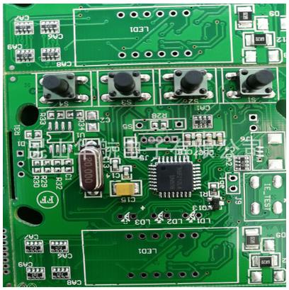
Components of similar types should be arranged on the board in the same direction to make the placement, inspection and soldering of the components easier.
For example, make the negative poles of all radial capacitors face the right side of the board, make the notch marks of all dual in-line packages (DIP) face the same direction, etc. This can speed up the insertion speed and make it easier to find errors.
Because the A board uses this method, it is easy to find the reverse capacitor, while the B board search takes more time.
In fact, a company can standardize the direction of all circuit board components it manufactures. Some board layouts may not necessarily allow this, but this should be a direction of effort.
What is the manufacturability of PCB design
Also, similar component types should be grounded together as much as possible, and the first pins of all components should be in the same direction.
What is the manufacturability of PCB design
But the author did encounter quite a lot of PCBs, the assembly density is too high, on the PCB welding surface must also be distributed with higher components such as tantalum capacitors, chip inductors and fine-pitch SOIC, TSOP and other devices, in this case, only Reflow soldering after double-sided printing solder paste patch can be used, and the plug-in components should be concentrated as much as possible in the component distribution to accommodate manual soldering.
Another possibility is that the perforated components on the component surface should be distributed on several main straight lines as much as possible to adapt to the latest selective wave soldering process, which can avoid manual soldering to improve efficiency and ensure soldering quality. Discrete solder joint distribution is a taboo for selective wave soldering, which will increase the processing time exponentially.
When adjusting the position of the components in the printed board file, you must pay attention to the one-to-one correspondence between the components and the silk-screen symbols. If the components are moved without correspondingly moving the silk-screen symbols next to the components, it will become a major quality hazard in manufacturing., Because in actual production, silk screen symbols are industry language that can guide production.
2. The PCB must be equipped with clamping edges, positioning marks, and process positioning holes for automated production. At present, electronic assembly is one of the industries with the highest degree of automation. The automation equipment used in production requires automatic transmission of PCBs. In the transfer direction of the PCB (usually the long side direction), there is a clamping edge not less than 3-5mm wide on the upper and lower sides to facilitate automatic transmission and prevent components near the edge of the board from being unable to be automatically assembled due to clamping.
The function of the positioning mark is that for the currently widely used optical positioning assembly equipment, the PCB needs to provide at least two to three positioning marks for the optical identification system to accurately position the PCB and correct the PCB processing errors.
Among the commonly used positioning marks, two marks must be distributed on the diagonal of the PCB. The selection of positioning marks generally uses standard graphics such as solid round pads. For easy identification, there should be an open area without other circuit features or marks around the mark. The size should preferably not be less than the diameter of the mark. The mark should be 5mm away from the edge of the board. above.