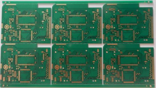
In fact, every electronic product currently produced is powered by one or more PCBs. In the past few years, designers have pushed the limits of these thin conductive materials to the limit, designing them to accommodate a range of integrated circuits and critical connections, as well as smaller size requirements. In order to keep up with these rapid developments, PCB assembly (PCBA) suppliers must conduct quality assurance testing to thoroughly check product quality and testing;
defect. Deficiencies in defining characteristics such as size and power consumption will not only directly affect the board on which it is located, but also endanger the entire manufacturing process and supply chain. In mass production, even occasional deformations can undermine the manufacturer's basic goals of achieving higher yields, lowering defect rates, and lowering costs.

PCBA suppliers cannot simply trust that suppliers-even reputable suppliers-will automatically perform quality assurance checks. They must also verify each part through their own inspections in order to provide original equipment manufacturers (OEMs) with the highest quality end-user product parts. At present, the most commonly used PCB quality inspection methods and tools are:
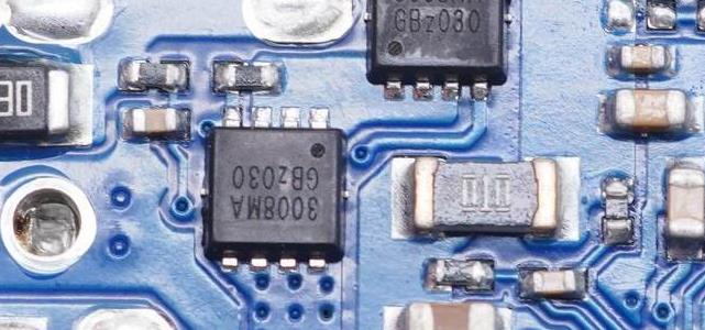
Vision-For small batch production runs, an effective form of inspection is for someone (usually the person performing the assembly) to see directly with their own eyes. This doesn't just mean quick browsing; they must carefully check every connection in a well-lit environment.
Microscope-In order to reduce the pressure on the eyes, the inspector can use hand-held optical tools, such as a magnifying glass or a jeweler's magnifying glass, to expand the field of view of the circuit board components. In order to observe more closely, they can use a USB microscope to project the PCB connection onto a large screen for detailed inspection.
In-circuit testing-capacitance testing includes two different electronic testing methods: bed of nails and no fixtures. The nail bed test consists of a series of small spring-loaded pins that can be pressed into different test points to measure resistance. No fixture or flying probe test sends the machine-operated probe to the PCB to check the test point at a very fast speed.
X-rays-Compared to photographs or microscopic images, X-rays provide a non-invasive, albeit expensive, method to visually inspect the correct PCB components. Sawing-Cutting a PCB with a saw is destructive to the veneer, but can provide valuable insights into the overall situation of the entire assembly process.
Automatic Optical Inspection (AOI)-AOI system is inexpensive and commercialized. Cheap AOI systems use a combination of cheap webcams and open source computer vision (openCV) to compare webcam PCB images with images of "perfect" circuit boards and identify inconsistencies or defects. Commercial AOI uses higher-quality cameras and RBG LEDs to reflect light to check connection failures and soldering quality. Functional test-This test method is basically a trial run after the PCB is manufactured. The operator opens the PCB and programs it to perform a series of self-checks.
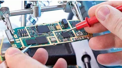
Check the camera-the preferred tool for PCB quality assurance. The inspection camera allows the operator to observe the ergonomics with the naked eye. These high-resolution camera images are projected onto the computer screen and manipulated to check microscopic details, and are easily shared with different departments for further inspection.
The floor staff who conduct the final PCB assembly inspection must receive training on some key quality control indicators to achieve the ultimate goal of improving reliability and reducing circuit board complexity and component count. The two effective quality standards are Defects Per Unit (DPU) and Defects Per Million Opportunities (DPMO). The former measures the number of defects on each circuit board, and the latter measures one million circuit boards of varying complexity. The normalization factor for the total number of defects. Through these two indicators, manufacturers can track the quality of products and processes.
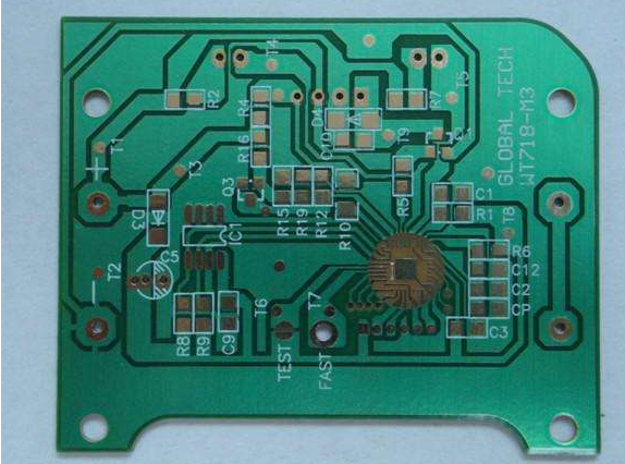
The lead engineer can also view the PCB layout and routing path to determine if any layers need to be added to optimize the circuit. You can add laminations as needed to balance the center of the sheet with respect to its z-axis. The final touch check includes confirming that the nodes and circuits do not have unnecessary noise, verifying whether there is a solder mask between the pins and vias, and ensuring that the screen printing of the circuit board is obvious to the user.