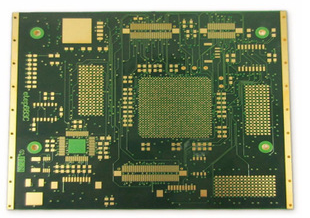
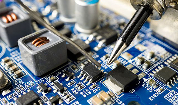
QFN (quad flat no leads) seems to have an increasingly common trend in IC packaging in the PCB industry. QFN has the advantages of small size, comparable to CSP (chip scale packaging), and relatively low cost. The yield rate of the IC production process is also quite high, and it can also provide better coplanarity and heat dissipation for high-speed and power management circuits. In addition, the QFN package does not require leads from four sides, so the electrical efficiency is better than the lead package. Traditional PCB packaged ICs, such as so with multiple pins, must be led out from the side.
Although QFN packaging has many electrical and application advantages, it has brought many soldering quality effects to PCB assembly plants. Due to the leadless design of QFN, it is usually difficult to judge whether its solderability is good from the solder joints on its appearance. Although there are still solder joints on the side of the QFN package, some IC package manufacturers only cut [lead frame] to expose it. The cutting part does not require electroplating, so it is basically not easy to eat tin on the QFN side. In addition, the cutting section is easily oxidized after storage for a period of time, which makes the tin on the side difficult to eat.

▼ The side solder foot of QFN is the cut part of the lead frame without electroplating coating.
QFN tin standard
In fact, in section 8.2.13 of the ipc-a-610d specification, the plastic quad flat package no-lead (pqfn) does not clearly stipulate that the side tin of the QFN must have a smooth arc curve.
Some package configurations do not expose solder toes, or there is no continuous solderable surface on the exposed solder toes on the outside of the package, and no toe fillets are formed.
In other words, QFN welding cannot use the welding conditions of the side of the pipe, as long as the bottom of the QFN solder leg and the position of the heat sink on the right bottom really corrode tin. The tin swallowing of the soldering feet at the bottom of the QFN can actually be imagined as BGA, so it is recommended to refer to the plastic BGA standard in section 8.2.12 of ipc-a-610d. The amount of tin plating on the middle ground pad may depend on the design of each PCB company.
▼ Although the solder pins on the QFN side are not conducive to attracting tin, their bottom surface has good tin absorption and electrical characteristics are still good.
▼ The solder feet on the side of the QFN are in good condition.
QFN solderability inspection and testing is the same as the solder inspection standard of BGA. At present, the solder inspection of QFN packages not only uses in-circuit testing and functional verification testing to test its function, but also usually uses optical instruments or X-rays to check the open circuit of its solder. And short circuit. To be honest, if the X-ray level is not good enough, it is really not easy to check the QFN welding problem. If solderability problems are found anyway, they can only be checked by destructive tests (such as micro-section or red dye penetration tests).
Possible solutions for QFN gas welding
When it is found that the QFN has empty soldering, it is necessary to clarify whether the parts have oxidation problems, take the parts for immersion tin test to confirm, and then judge whether there are empty soldering problems in the fixed solder feet. Under normal circumstances, the grounding pins are prone to empty soldering. You can consider changing the wiring design of the circuit board and adding heat dissipation pads on the circuit board traces to reduce the proportion of the solder pins directly grounded. This will delay the heat loss speed ( The so-called "thermal resistance" refers to reducing the width of the grounding wire so that the heat energy will not be transmitted to the entire grounding copper strip immediately.) You can also try to adjust the furnace temperature (reflow curve) or change to the slope reflow type to reduce preheating The problem of excessive heat absorption of solder paste during this period.
Reference reading: reflux curve
It was found that there was too much solder paste printed on the ground pad at the bottom of the QFN, which caused the parts to float during the reflow soldering process, forming an empty solder. At this time, it can be considered that in the shape of the "field", printing the ground pad at the bottom of the QFN is better than printing the entire workpiece, and because all the solder paste melts into balls during the reflow soldering process, it is unlikely to cause parts Float.
Reference reading: The processing principle of the through hole in the pad
In addition, try not to set the through holes on the PCB pad, and plug the through holes on the middle heat dissipation ground pad as much as possible, otherwise it will easily affect the quantity
Reference reading: The processing principle of the through hole in the pad
In addition, the through holes on the PCB pads should not be set as much as possible, and the through holes on the middle heat dissipation ground sheet should be blocked as much as possible, otherwise it will easily affect the amount of solder and generate bubbles, which may lead to poor soldering in severe cases.