The basic principles of wiring of high-speed PCB signal lines
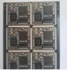
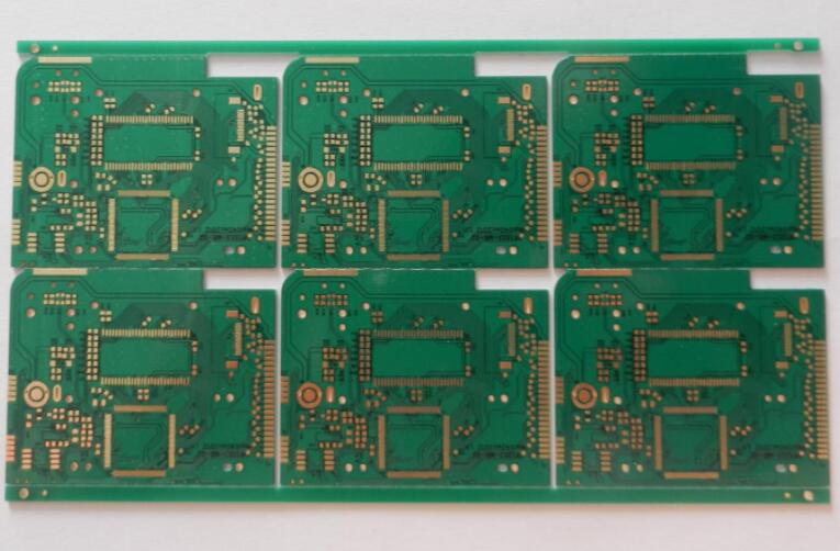
(1) Reasonable selection of the number of layers: High-frequency circuits tend to have high integration and high wiring density, so multilayer boards must be used for wiring, which is also an effective means to reduce interference. Reasonable selection of the number of layers can greatly reduce the PCB size, make full use of the intermediate layer to set up the shield, better realize the nearest grounding, effectively reduce the parasitic inductance, effectively shorten the signal transmission distance, and greatly reduce the crossover between signals Interference etc. All these beeps are conducive to the reliable operation of high-frequency circuits. Some data show that the noise of a 4-layer board of the same material is 20dB lower than that of a double-sided board, but the higher the number of layers, the more complicated the manufacturing process and the higher the cost.
(2) Reduce the bending of the leads between the pins of high-speed circuit components: The leads of high-frequency circuit wiring are best to be fully straight. If you need to bend, you can use a 45° fold line or a circular arc line, which can reduce the external emission and mutual coupling of high-frequency signals.
(3) Shorten the leads between the pins of high-frequency circuit components: The most effective way to meet the shortest wiring is to make a wiring appointment for key high-speed networks before automatic wiring.
(4) Reduce the overlap between the lead layers between the pins of high-frequency circuit components: the so-called reduction of the overlap between the layers of the leads refers to the reduction of the vias used in the connection of the components. One via can bring about 0.5pF distributed capacitance, and reducing the number of vias can significantly increase the speed.

(5) Pay attention to the cross interference introduced when the signal lines are wired in parallel at close distances: If the parallel distribution cannot be avoided, a large area of ground wire can be arranged on the opposite side of the flat tooth stripping signal line to greatly reduce the interference. Parallel wiring in the same layer is almost unavoidable, but the wiring directions of two adjacent layers must be perpendicular to each other. In high-frequency circuit wiring, it is best to conduct horizontal and vertical wiring in adjacent layers. When parallel wiring in the same layer cannot be avoided, a large-area ground wire can be laid on the reverse side of the PCB to reduce interference. This is for the commonly used double-sided board. When using a multilayer board, the power layer in the middle can be used to achieve this function. The copper-clad PCB board can not only improve the high frequency anti-interference ability, but also has great benefits for heat dissipation and increase the strength of the PCB. In addition, if tin-plated grids on the PCB fixing openings on the metal chassis can not only improve the fixing strength and ensure good contact, but also the metal chassis can be used to form a suitable common line.
(6) Implement ground wire surround measures for particularly important signal lines or local sound bullet elements. Partially packet processing of clocks and other units is very beneficial to the creation of high-speed systems.
(7) Various signal wirings cannot form loops, nor can they form current loops.
(8) A high-frequency decoupling capacitor should be installed near each integrated circuit block.
Ground wire design
Ground wire design In electronic equipment, an important method of controlling interference is grounding. If you can correctly combine the shielding of the wings and the mouth, you can solve most of the interference problems. In electronic equipment, the ground structure roughly includes system ground, chassis ground (shield ground), digital ground (logical ground), and analog ground. Pay attention to the following 4 points in the ground wire design.
1) Correctly choose single-point grounding and multi-point grounding. In false whisker circuits, the operating frequency of the signal is usually less than 1MHz, and the inductance between wiring and components has less impact, while the ring tree formed by the grounding circuit has a greater impact. One point grounding method should be used. When the signal operating frequency is greater than 10MHz, the ground wire impedance will become very large. At this time, the ground wire impedance should be reduced as much as possible, and the nearest multi-point grounding method should be adopted. When the working frequency is 1~10MHz, if one-point grounding is adopted, the ground wire length should not exceed 1/20 of the wavelength, otherwise, multi-point grounding should be adopted.
2) Divide the digital circuit from the analog circuit. When there are both high-speed logic circuits and linear circuits on the PCB, they should be separated as much as possible. The ground wires of the two should not be mixed, and they should be connected to the ground wires of the power supply. Try to increase the grounding area of the linear circuit as much as possible.
3) Thicken the grounding wire as much as possible. If the grounding wire is very thin, the grounding electricity will change with the change of the current, which will cause the timing signal level of the electronic equipment to be unstable and the anti-noise performance to deteriorate. Therefore, the mausoleum ground wire should be thickened as much as possible so that it can pass 3 times the allowable current of the PCB. If possible, the width of the ground wire should be greater than 3mm.
4) When the ground wire is formed into a closed loop, when designing a PCB ground wire system composed of only digital circuits, the ground wire should be designed as a closed loop, which can significantly improve the anti-noise ability. The reason is that there are many integrated circuit components in the PCB design, especially when there are components that consume more power, due to the limitation of the thickness of the ground wire, a large potential difference will be generated on the ground wire, resulting in anti-noise ability decline. If the ground wire is formed into a loop, the potential difference will be reduced, thereby improving the anti-noise capability of electronic equipment.