PCB multi-layer circuit boards are usually defined as 10-20 or higher multi-layer boards, which are more difficult to process than traditional multi-layer boards and require high quality and high reliability. Mainly used in communication equipment, high-end servers, medical electronics, aviation, industrial control, military and other fields. In recent years, the market demand for advanced boards in communications, base stations, aviation, military and other fields has remained strong.
With the rapid development of China's communications equipment market, the high-rise board market has a bright future.
At present, high-level PCB proofing can be produced in large quantities from foreign-funded enterprises or a few domestic enterprises in China. The production of high-level circuit boards not only requires substantial investment in technology and equipment, but also requires the experience of technicians and manufacturers.

At the same time, customer certification procedures for multilayer circuit boards are more stringent and cumbersome. Therefore, the barriers for high-level circuit boards to enter the enterprise are very high, and the industrial production cycle is long.
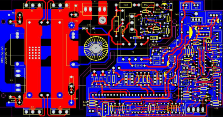
The average level of PCB has become an important technical indicator to measure the technical level and product structure of PCB companies. This article briefly introduces the main processing difficulties encountered in the production of advanced circuit boards, and introduces the key production technology control points of multilayer circuit boards for reference. Compared with traditional PCB products, advanced PCB has the characteristics of thick board, multilayer, dense lines, multiple through holes, large unit size, thin middle layer, etc., requiring larger internal space, layer alignment, impedance control and reliability sex.
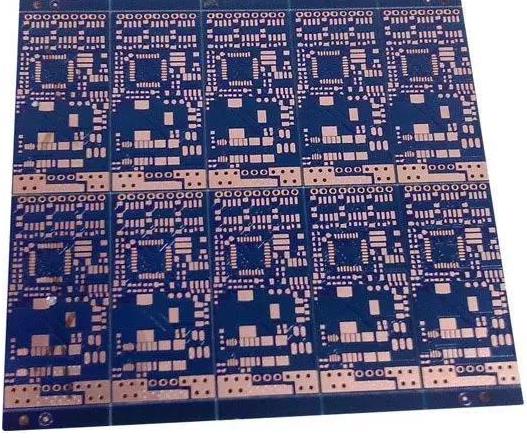
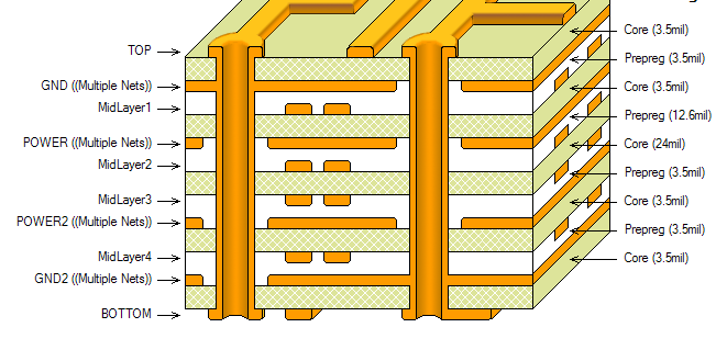
PCB multilayer board production
1: Difficulty of alignment between layers
Due to the large number of mid-level panels, users have increasingly higher requirements for the calibration of the PCB layer. Generally, the alignment tolerance between the layers is controlled at 75 microns. Taking into account the large size of the high-rise board unit, the high temperature and humidity of the graphics conversion workshop environment, the misalignment and overlap caused by the inconsistency of different core boards, the positioning method between layers, etc., make control possible. The middle high-rise board is more difficult.
2: Difficulty in making internal circuits
The high board uses special materials such as high TG, high speed, high frequency, thick copper, thin dielectric layer, etc., which puts forward high requirements for the production of internal circuits and the control of pattern size. For example, the integrity of impedance signal transmission makes it more difficult to manufacture internal circuits.
Width and line spacing are small, open circuit and short circuit increase, short circuit increase, low pass rate, fine line signal layer, internal AOI leakage detection probability increases, internal core board is thin, easy to wrinkle, poor exposure, easy to curl the etching machine; advanced refers to More system boards, larger unit sizes and higher product scrap costs.
3: Compress PCB manufacturing difficulties
Many inner core boards and semi-cured boards are stacked together, which are prone to defects such as sliding plates, delamination, resin voids and bubble residues in the stamping production. In the design of the laminated structure, the heat resistance, pressure resistance, glue content and dielectric thickness of the material should be fully considered, and a reasonable high laminate plan should be formulated. Due to the number of layers, expansion and contraction control and size factor compensation cannot be kept consistent, the thin insulating layer can easily lead to failure of the interlayer reliability test.
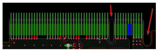
4: Difficulty in drilling
The use of special boards with high TG, high speed, high frequency and thick copper increases the PCB drilling roughness, drilling burrs and the difficulty of drilling. There are many layers, the cumulative total copper thickness and the plate thickness, the drill bit is easy to break, there are many compact BGAs, and the narrow hole wall spacing will cause the CAF failure problem, because the plate thickness can easily lead to the problem of slant drilling.