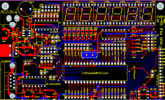
Double-sided PCB board manufacturing process
In recent years, the typical methods for manufacturing double-sided metalized printing plates are the SMOBC method and the pattern plating method. In some cases process conductors are also used.
1. Graphic electroplating process:
Foil board - blanking - drilling front edge hole - CNC drilling - inspection - deburring - electroless thin copper plating - thin copper electroplating - inspection - brushing - film (or screen printing) - exposure and development (or curing) - inspection Repair board-graphic plating (Cu(Sn/Pb))-film removal-etching-test and repair board-nickel-plated plug-hot melt cleaning-electrical continuity detection-cleaning treatment-mesh seal resistance welding pattern-curing-screen printing mark Symbol - curing - shape processing - cleaning and drying - inspection - packaging - finished product.

In this method, the two processes of "electroless copper plating and electroless copper plating" can be replaced by the process of "electroless copper plating", both of which have advantages and disadvantages. The pattern plating-etching method of double-sided metallization is a typical process in the 1960s and 1970s. In the 1980s, bare copper coated solder film (SMOBC) gradually developed, especially in precision double-sided panel manufacturing has become the mainstream process.
2. SMOBC process:
The main advantage of the SMOBC board is that it solves the short circuit of the solder bridge between the thin wires, and because the lead-to-tin ratio is constant, it has better solderability and storage properties than the hot melt board. There are many methods of manufacturing SMOBC boards, including standard pattern plating of smobC process that subtracts back-blade lead-tin, using tin-plated or immersion tin instead of electroplated lead-tin minus patterned plating of SMOBC process plating holes, plugging holes or mask holes SMOBC process, additive SMOBC process.
The following mainly introduces the sMOBC process of the pattern plating method, the tin stripping process of lead-tin and the sMOBC process of the blocking hole method.
1. Pattern electroplating method and back lead-tin L process:
The SMOBC process method of pattern plating and re-degradation of lead and tin is similar to the pattern plating process. Change only after etching.
Double-sided copper foil board, according to the pattern plating process to the etching process, de-lead tin, inspection, cleaning, soldering graphics, plug nickel plating-plug sticking tape, hot air leveling, cleaning, grid marking symbols, shape processing, cleaning and drying, Finished product inspection, packaging, finished product.
2. The main process of plugging method is as follows:
Double-sided aluminum foil board-drilling-electroless copper plating-copper plating on the whole board-plug hole-reticulated imaging (positive image)-etching-removing mesh material-removing clogging material-cleaning-welding pattern-plug nickel plating-gold plating Adhesive tape - hot air leveling - processing and finished products.
The process steps of this PCB production process are relatively simple, and the key is the ink that plugs and washes the holes.
If the hole blocking ink is not used in the process of blocking holes and grid imaging, and a special masking dry film is used to cover the holes, and then exposed to make a portrait figure, this is the process of masking the holes. Compared with the hole blocking method, there is no longer the problem of cleaning the ink in the hole, but there is a higher requirement for the cover of the dry film.
The basis of the SMOBC process is to produce a metallized bare copper double-sided board on the PCB, and then apply a hot air leveling process.