One, common mistakes in the schematic diagram of the PCB board
(1) ERC reports that the pin has no access signal:
a. Define the I/O attributes of the pins when creating the package;
b. When creating a component, the pin direction is reversed and must be connected to the non-pin name end;
C. Inconsistent mesh properties were modified when components were created or placed, and the pins were not connected to the pipeline.
The most common reason is that there is no engineering documentation. This is the most common mistake that beginners make:
(2) The PCB component runs outside the boundary of the engineering drawing: no component is created in the center of the component library chart paper;
(3) When using a component that creates a multi-part component, do not use the table name;
(4) The created project file netlist can only be partially adjusted to PCB: the global list is not selected when the netlist is generated.
Second, common mistakes of PCB board

(1) Report that NODE was not found during network loading:
a. The components in the schematic diagram are used in software packages that are not available in the PCB library;
b. The components in the schematic diagram are packaged with inconsistent names in the PCB library;
C. The components in the schematic diagram are inconsistent with the software packages in the PCB library.
Such as sanso: the pin numbers in the sss are e, b, c, and the numbers on the PCB board are 1, 2, 3.
(2) Cannot always print on paper when printing
a. The PCB library is not created in the original location;
b. The component will move and rotate many times, and its hidden characters will exceed the boundary of the PCB board. Choose to show all hidden characters, shrink the PCB, and then move the characters within the boundary.
(3) Congo (DRC) reported that the network has been divided into several parts
Indicates that the network is not connected. Please check the report file and use the "CONNECTEDCOPPER" option to find out. If the design is more complicated, please try not to use automatic routing.
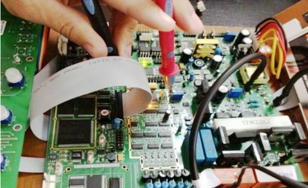
Three, common mistakes in the PCB manufacturing process
After years of practice and exploration, Shenzhen Zhongke Circuit Technology Co., Ltd., as a professional PCB circuit board supplier, focuses on high-precision double-sided/multi-layer circuit board factories, HDI boards, thick copper boards, blind buried boards, high frequency Circuit board production and PCB sampling, as well as the production and manufacturing of small and medium-sized batch processing boards. Over the years, he has been focusing on the production of multi-layer precision circuit boards. Technical Manager Li has always shared with us some experience in the perfect integration of PCB manufacturing and design.
(1) Pad overlap
a. Causes heavy holes, drilling multiple times in the same area will damage the drill bit and holes;
b. On the multi-layer board, there are two connecting plates at the same position and one isolation plate, which makes the board perform well. Isolation, wrong connection.
(2) Irregular use of graphics layer
a. Violation of conventional design, such as the surface design of the bottom part and the welding surface design of the TOP layer, will cause misunderstanding;
b. There are many design wastes on each layer, such as polylines, useless borders, labels, etc.
(3) Unreasonable personality
a. The characters cover the SMD solder tabs, which brings inconvenience to PCB inspection and component soldering;
b. If the characters are too small, it will be difficult to screen printing. If the characters are too large, the characters will overlap each other and be difficult to distinguish. The font is generally 40mil.
(4) Single-sided pad setting hole
a. A. Single-sided pads are usually not drilled, and the hole diameter should be designed to be zero, otherwise, when the drilling data is generated, the hole should be drilled at this position;
b. If it is necessary to drill a single-sided pad in the output of electrical and ground data, instead of designing the aperture, the software will use the PCB pad as the SMT pad and discard the inner layer of the isolation disk.
(5) Draw a pad with padding edge blocks
This allows the DRC to pass the DRC inspection, but the soldering data cannot be directly generated during the processing, so the solder-resistant pad cover cannot be soldered.
(6) The electrical stratum is designed with a cooling plate and a signal line at the same time, and the image and the negative image are designed together, and there is an error.
(7) Large area grid spacing is too small
The grid line spacing is 0.3mm. During the PCB manufacturing process, the broken film development after the development during the pattern transfer process is caused by the broken line.
(8) The graphics are too close to the outer frame
Ensure that there is at least 0.2mm spacing (more than 0.35mm when V-shaped cutting), otherwise the outer layer will raise the copper foil and prevent the flux from falling. Affect the appearance quality (including the copper layer of the inner layer of the multilayer board).
(9) Unclear frame design
There are many and inconsistent design layers of the frame, which makes it difficult for PCB manufacturers to judge which line is formed. The standard frame should be designed on the mechanical layer or the BOARD layer, and the internal hollow part should be clear.
(10) Uneven graphic design
When pattern plating occurs, the current distribution is uneven, which affects the uniform coating and even causes warpage.
(11) Short special holes
The length/width of the special hole should be 2:1 and the width should be 1.0mm, otherwise the CNC drill will not be able to be processed.
(12) Undesigned milling shape positioning hole
If possible, design at least 2 positioning holes with a diameter of 1.5mm on the PCB board.
(13) The aperture mark is not clear
a. Combine as many holes as possible into the storage area where the holes can be combined;
b. The aperture label should be marked in metric system as much as possible, and add 0.05;
c. Are the tolerances of metallized holes and special holes (such as crimp holes) clearly marked?
(14) The inner layer of the multilayer circuit board is unreasonable
a. There are gaps in the design of the isolation zone, which is easy to cause misunderstanding;
b. The design of the isolation zone is too narrow to accurately judge the network;
c. The thermal pad is placed on the spacer, and the hole is prone to poor connection.