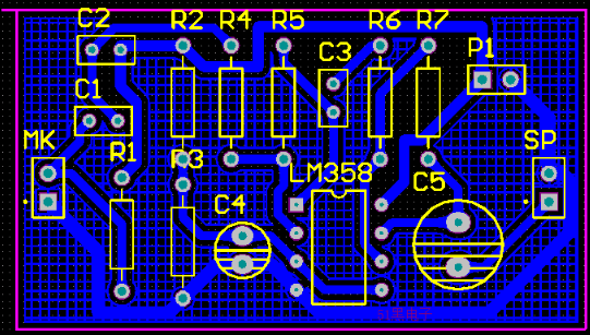
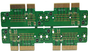
Layout is one of the most basic skills of PCB design engineers. The quality of wiring will directly affect the performance of the whole system. Most high-speed design theories will finally be realized and verified through layout. Therefore, wiring is very important in high-speed PCB design. The following will analyze its rationality and give some optimized routing strategies for some situations that may be encountered in the actual wiring. Mainly from the right angle routing, differential routing, serpentine line and other three aspects.
1. Right angle routing
Right angle routing is generally required to be avoided in PCB wiring, and it has almost become one of the standards to measure the quality of wiring. How much impact will right angle routing have on signal transmission? In principle, right angle routing will change the linewidth of the transmission line, resulting in discontinuity of impedance. In fact, not only right angle routing, dun angle and acute angle routing may cause impedance change.
The influence of right angle routing on the signal is mainly reflected in three aspects: first, the corner can be equivalent to the capacitive load on the transmission line to slow down the rise time; Second, the discontinuous impedance will cause the reflection of the signal; The third is the EMI generated by the right angle tip.
The parasitic capacitance caused by the right angle of the transmission line can be calculated by the following empirical formula:
C=61W(Er)[size=1]1/2[/size]/Z0
In the above formula, C refers to the equivalent capacitance of the corner (unit: PF), and W refers to the width of the wiring (unit: inch), ε R refers to the dielectric constant of the medium, and Z0 is the characteristic impedance of the transmission line. For example, for a 4mils 50 ohm transmission line( ε R is 4.3), the electric capacity brought by a right angle is about 0.0101pf, and then the rise time change caused by it can be estimated:
T10-90%=2.2*C*Z0/2 = 2.2*0.0101*50/2 = 0.556ps

Through calculation, it can be seen that the capacitance effect caused by right angle routing is extremely small.
As the linewidth of the right angle line increases, the impedance will decrease, and a certain signal reflection phenomenon will occur. We can calculate the equivalent impedance after the linewidth increases according to the impedance calculation formula mentioned in the transmission line chapter, and then calculate the reflection coefficient according to the empirical formula:
ρ= (zs-z0) / (ZS + Z0). Generally, the impedance change caused by right angle wiring is between 7% - 20%, so the maximum reflection coefficient is about 0.1. Moreover, as can be seen from the figure below, the impedance of the transmission line changes to the minimum within a long time of the w / 2 line, and then returns to the normal impedance after the w / 2 time. The whole time of impedance change is very short, often within 10ps. Such a fast and small change is almost negligible for general signal transmission.
Many people have this understanding of right angle routing and think that the tip is easy to transmit or receive electromagnetic waves and generate EMI, which has also become one of the reasons why many people think that right angle routing cannot be used. However, the results of many practical tests show that right angle routing does not produce obvious EMI than straight line. Perhaps the current instrument performance and test level restrict the accuracy of the test, but at least it shows a problem that the radiation of right angle routing is less than the measurement error of the instrument itself.
Generally speaking, the right angle routing is not as terrible as expected. At least in applications below GHz, any effects such as capacitance, reflection and EMI can hardly be reflected in TDR test. High speed PCB design engineers should focus on layout, power / ground design, wiring design, vias and other aspects. Of course, although the impact of right angle wiring is not very serious, it does not mean that we can take right angle wiring in the future. Paying attention to details is a necessary basic quality for every excellent engineer. Moreover, with the rapid development of digital circuits, the signal frequency processed by PCB engineers will continue to increase to the RF design field above 10GHz, These small right angles may become the focus of high-speed problems.
PCB Differential routing
Differential signal is more and more widely used in high-speed circuit design. The most critical signal in the circuit often adopts differential structure design. What makes it so popular? How can we ensure its good performance in PCB design? With these two questions, we will discuss the next part.
What is differential signal? Generally speaking, the driver sends two equivalent and inverted signals, and the receiver judges whether the logic state is "0" or "1" by comparing the difference between the two voltages. The pair of routing lines carrying differential signals is called differential routing.