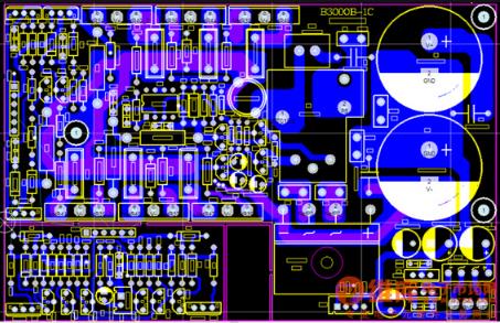
How to make the power loop in the PCB circuit board. I have done a few years of power board layout, and summarized some main areas of concern, mainly from the following points to consider:
1, the Power loop part
More importantly, the power board must first bear the power loop part. In the PCB layout, you should first know the circuit characteristics of the power part. The power supply circuit is mainly divided into Di / dt circuit and DV / DT circuit. There are two lines when walking. The layout is different.
Since the DI/DT circuit is relatively large when the current changes per unit time, the loop area of the entire circuit should be as small as possible when this part of the circuit is in the circuit. The loop area is the smallest, and the interference itself can be coupled off. The focus of the DV / DT circuit is completely different, because this circuit will have a relatively large voltage change per unit time, so it is easy to cause external interference, so the copper skin of this circuit should not be too wide when it is in the circuit. It can meet the bearing current copper skin When the width is as small as possible, the overlapping area of different layers is as small as possible, and the sensitive signals in the PCB copy board are as far away as possible from these lines. How to make the power loop in the PCB circuit board?

2 the line of the driving part of the driving part should first consider the area of the entire driving ring, as small as possible to keep away from the interference source and as close to the driving part as possible.
Under the driving of power components such as MOS tube, the wiring of the G pole and the D pole should not be parallel when routing, because in most cases, the D pole part of the MoS tube is a DV / DT circuit, G The pole is the drive circuit. If you connect in parallel, the drive signal is easily interfered. As a result
III. Sampling signal Sampling signal Sampling signal and current sampling are also very important in the power supply board, because they are directly related to the control terminal. All these sampling signals must avoid other signals as much as possible. If possible, the sampling signals can be sampled differently. And in the corresponding wiring position can give them a complete ground plane.
Two, several points of attention in PCB copy board layout
Pay attention to several points of PCB copy board layout, not to mention the importance of the ground, no matter what kind of board, the treatment of the ground is very important. It is more complicated on the power board, because the power supply part of the ground is many times, and the small current of the control part is very common, so it is very important to deal with these places this time. In my experience dealing with these places, the key is to choose the correct single-point connection The node, because the design of each power supply is different, so the single-point connection point selection is also different. I generally choose a bus capacitor and a ground pin in low-power photovoltaic inverters. Inverter I is generally a capacitor. Under the large current of the ground pin capacitance, to the switching power supply input end of the capacitor on the pin, and then from this ground pin to the switching power supply behind the small current on the ground plane, of course there are other places, such as crystal vibration, Ground sampling, etc., each company has different design rules and methods, and there are more ground information processed online.
Fifth, safety regulations Safety in the design of power supply products is indispensable. There are also differences in the corresponding safety regulations of different countries in different regions, and the application of environmental pollution levels and altitude will have a greater impact. To master the safety distance, all of us must understand these factors at the beginning of the design. If there are safety engineers, you can ask them to give a more professional distance between crawling and electrical clearance. We actually need to pay special attention to those in PCB layout Metal components in the PCB area, such as a fuse, whose middle metal is non-metallic. If there is no seat, the two metals of the fuse will be in contact with the PCB. All surface lines around the fuse should be careful to avoid these metal areas.
Six, heat dissipation
For those systems with relatively large power, heat dissipation is also very important. This general situation and structure are good. Before designing, understand the overall structure of the heat dissipation mode. It is natural cooling, air cooling or water cooling, of which air cooling and suction Blown, these will have a relatively large impact on the layout.
seven. Electromagnetic compatibility (EMC) mainly means that some power supply parts of the line width should not be mutated as much as possible. If corners are needed, the corners should be made as smooth as possible and not mutated. Sometimes there are large currents and small currents. Some sampled signals may be connected to the network. Shared, but when the lines are not shared, they must be separated, and it is best to go to each loop.