In fact, the printed circuit board (PCB) is composed of wire-like materials, that is, its impedance should be constant. So why does PCB introduce nonlinearity into the signal?
The answer is: the position of the PCB layout relative to the current flow is "spatially nonlinear". Whether the amplifier draws current from this power supply or another power supply depends on the instantaneous polarity of the signal on the load. The current flows out of the power supply, passes through the bypass capacitor, and enters the load through the amplifier.
Then, the current returns from the load ground (or shielded from the PCB output connector) to the ground plane, passes through the bypass capacitor and returns to the power source that originally provided the current. The concept of the path of least current flowing through impedance is incorrect. The amount of current in all different impedance paths is proportional to their conductivity. In the ground plane, there is usually a low impedance path through which a large proportion of current flows: one path is directly connected to the bypass capacitor, and the other path excites the input resistor before reaching the bypass capacitor.

The ground return current is the real cause of the problem.
Measures to reduce harmonic distortion in PCB design When bypass capacitors are placed in different positions on the PCB, the ground current flows through different paths of the corresponding bypass capacitors, which means "spatial nonlinearity". If most of the components of a certain polarity of the ground current flow through the ground of the input circuit, only the component voltage of the signal of that polarity will be disturbed. If the other polarity of the ground current is not disturbed, the input signal voltage changes in a non-linear manner. When one polarity component changes and the other polarity does not change, it will produce distortion and appear as two-harmonic distortion of the output signal.
Measures to reduce harmonic distortion in PCB proofing design When only one polarity component of the sine wave is disturbed, the generated waveform is no longer a sine wave. Use a 100ω load to simulate an ideal amplifier, make the load current pass through a 1ω resistor, and only the input ground voltage is coupled to one polarity of the signal, and the result shown in Figure 3 is obtained. The Fourier transform shows that the distorted waveforms are almost all two harmonics of -68DBC. When the frequency is very high, it is easy to produce this degree of coupling on the PCB, which can destroy the excellent anti-distortion characteristics of the amplifier without requiring too many special non-linear effects of the PCB.
When the output of a single operational amplifier is distorted by the ground current path, the bypass loop can be rearranged to adjust the flow of ground current and keep the distance from the input device
Measures to reduce harmonic distortion in PCB proofing design
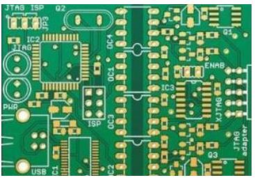
Multi-amplifier chips The problem of multi-amplifier chips (two, three or four amplifiers) is more complicated because it does not allow the ground connection of the bypass capacitor to be far away from all inputs. The problem of attention to printed wires when PCB proofing is especially true for quad amplifiers.
Each side of the four-way amplifier chip has an input terminal, so there is no space for a bypass circuit, which can reduce the interference to the input channel.
Measures to reduce harmonic distortion in PCB design Figure 5 shows an easy way to lay out four amplifiers. Most devices connect directly to the four amplifier pins. The ground current of one power supply will interfere with the input ground voltage and ground current of the other channel power supply, resulting in distortion. For example, the (+VS) bypass capacitor on channel 1 of the quad amplifier can be placed directly near its input, while the (-VS) bypass capacitor can be placed on the other side of the package. (+VS) ground current may interfere with channel 1, while (-VS) ground current may not.