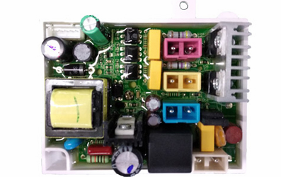
Printed circuit boards manufacturers are under significant pressure to increase density, reduce footprint, reduce side size, manage heat flow, and improve data rates while improving reliability and reducing costs. As they succeeded in reducing these pressures, an interesting challenge arose for designers to align multiple pairs of connectors between two PCBs.
What we need are clear guidelines to understand how to address these alignment challenges without sacrificing system performance, density, and reliability, while meeting increasingly stringent budget and time-to-market requirements.
This article discusses the alignment challenges in more detail before describing the conflicting requirements that can be encountered between advanced PCBs and more reliable high-density connectors so that these requirements can be efficiently met using design practices.

Miniaturization makes alignment of connectors difficult
There are a number of areas where PCB boards can be improved, including density, higher data rates, thermal management, and reliability. However, these improvements are accompanied by the pressure that the trend toward miniaturization puts on designers in the choice and implementation of connectors, especially pairing multiple connectors onto a PCB board.
In the case of connectors, miniaturization has resulted in a drop in spacing from 0.100 in. (2.54 mm) to 0.016 in. (0.40 mm) over the past 25 years -- a six-fold reduction that requires tighter tolerances. However, the tighter tolerances themselves are not the problem, but the variability around the nominal tolerances: if multiple connectors change to any of the nominal limits, some problems are more likely to occur.
An unlimited number of connectors can be successfully deployed between two PCBs provided that sandwich connectors and sufficiently rigid PCB boards can be manufactured, machined, and assembled in nominal conditions; In fact, tolerances and variability of material properties are limiting or determining factors. In the case shown in Figure 2, the designer needs to consider and account for tolerances for all components, including the often overlooked but related tolerances of (A) and (B) two PCB boards.
How to solve PCB board to the connector alignment problem
The purchase of some PCBs is controlled only by specifications embedded in Gerber packets. PCB boards can be fabricated from these data packets without mechanical tolerances.
For multi-connector applications, this package must be accompanied by separate mechanical drawings to indicate original drawing, drilling, and wiring tolerances.
At this point, designers need to do two things to help ensure a successful outcome. The first step is to find out what support PCB and connector vendors can provide to ensure alignment. The second is to ensure that system-level tolerance studies have been conducted to determine the alignment deviation of the connector resulting from its design. For A multi-connector sandwich card system consisting of A through F components, the connector supplier can only control the tolerance of the connector. A good supplier will meet or exceed published performance specifications, make PCB board tolerances and machining recommendations, and even provide reference recommendations for recommended PCB suppliers and equipment as needed.
The system or product designer should refer to the connector placeholder size and product specifications. Alignment deviation specifications included in these documents should be compared with the results of system-level tolerance studies to help ensure that multiple connectors between the same board are used successfully.
The connector system works as long as the initial and final angles and linear alignment deviations are not exceeded. These alignment deviations are calculated by taking into account factors such as insulator interference, beam deflection and contact friction. Exceeding alignment deviation values may result in circuit and/or insulator disconnection or damage.
While all necessary information such as design, component tolerances, equipment, and manufacturing capabilities is usually readily available to the designer, it is important to be able to contact the connector manufacturer to provide more specific guidance and validation of the alignment deviation tolerance buildup.
Positioning pins are not suitable for multi-connector applications
Some connector manufacturers offer optional positioning pins, usually on opposite sides of the bottom of the connector (Figure 4). These pins facilitate manual placement, can be used to help the connector orientation on the PCB, and do not add to the overall tolerance accumulation for single-connector applications.