With the increase of PCB wiring signals, electromagnetic compatibility (EMC) design is an issue that our electronic engineers must consider.
Faced with electromagnetic compatibility (EMC) design, when performing electromagnetic compatibility (EMC) analysis of products and designs, the following five important attributes need to be considered:
(1) Key device size: the physical size of the emitting device that generates radiation. The radio frequency (RF) current will generate an electromagnetic field, which will leak through the chassis and be separated from the chassis.
(2) Impedance matching:
The impedance of the source and receiver, and the transmission impedance between the two.
(3) Time characteristics of interference signal:
The problem is whether it is a continuous (periodic signal) event or just a specific operating cycle (for example, single-button operation or power-on interference, periodic disk drive operation, or network burst transmission).

(4) Interference signal strength:
How strong the energy level of the source is and how much potential it has to cause harmful interference.
(5) Frequency characteristics of interference signal:
The PCB proofing uses a spectrometer to observe the waveform, and observe the problem of the position of the spectrum, which is convenient to find the position of the problem. In addition, you also need to pay attention to some low-frequency circuit design habits. For example, my usual single-point grounding is ideal for low-frequency applications, but later I found that it is not suitable for RF signal applications because there are more EMI problems in the case of RF signals.
It is believed that some PCB engineers apply single-point grounding to all product designs without realizing that using this grounding method may lead to more or more complicated electromagnetic compatibility (EMC) issues. We should also pay attention to the current in the circuit components. Understanding the circuit Shenzhen PCB proofing, we know that the current flows from the high level to the low current, and the current always flows through one or more paths in the closed loop circuit, so it is the smallest loop and a very important rule. For those measured in the direction of the interference current, the PCB wiring is modified so that it does not affect the load or sensitive circuits.
Applications that require a high impedance path from the power supply to the load must consider all possible paths through which the return current can flow. There is also the problem of PCB wiring. The impedance of the wire or wiring includes resistance r and inductance, high frequency impedance and no tolerance. When the wiring frequency exceeds 100kHz, the wire or wiring becomes inductance. The wire or wiring that operates above the audio can become an RF antenna.
Shenzhen PCB proofing in the electromagnetic compatibility (EMC) specification does not allow wires or wiring to work below λ/20 of a specific frequency (the design length of the antenna is equal to Λ/4 or Λ/2 of the specific frequency), and when accidentally designed, The wiring becomes a high-performance antenna, which makes future debugging more difficult.
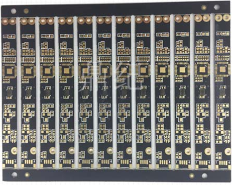
PCB layout issues:
First, consider the size of the PCB.
When the size of the PCB is too large, as the circuit grows, the anti-interference ability of the system is reduced, and the cost increases, and the size is too small to easily cause heat dissipation and mutual interference problems.
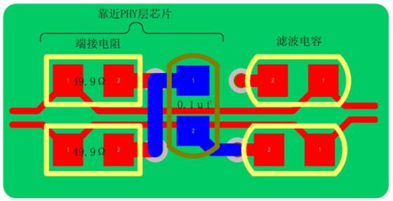
Second, determine the location of special components.
Such as clock components, it is best not to lay clock lines and not move up and down on key signal lines to avoid interference.
Third, according to the circuit function, the PCB as a whole is laid out. In the PCB component layout, the related components are as close as possible, so that a better anti-interference effect can be obtained.