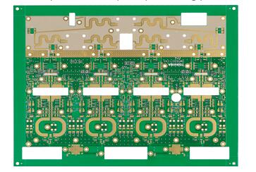
How to design the RF PCB small signal amplifier? The introduction is as follows:
In wireless communication systems, the level of the radio frequency signal reaching the receiver is mostly on the order of microvolts. Therefore, it is necessary to amplify weak radio frequency signals. The radio frequency small signal amplifier circuit is an important part of the wireless communication receiver. In most cases, the signal is not of a single frequency, but a frequency band signal that occupies a certain spectral width. In addition, because in the same channel, there may be many interference signals deviating from the useful signal frequency at the same time, so the radio frequency small-signal amplifying circuit must have a frequency selection function in addition to the amplifying function. RF small-signal amplifier circuits are divided into two categories: narrow-band amplifier circuits and wide-band amplifier circuits. Since the narrow-band amplifier circuit needs to amplify the weak signals with a center frequency of hundreds of kilohertz to hundreds of megahertz (or even a few gigahertz) and a bandwidth of several kilohertz to tens of megahertz without distortion, it is not only necessary There is a certain voltage gain and the ability to select frequency is required.

The narrow-band amplifier circuit uses active devices such as bipolar transistors, field effect tubes or radio frequency integrated circuits to provide voltage gain, and uses LC resonant circuits, ceramic filters, quartz crystal filters or surface acoustic wave filters to achieve frequency selection. .
Because the wide-band amplifier circuit needs to amplify the weak signal in a wide frequency band from several megahertz to several hundred megahertz (or even several gigahertz) without distortion, the amplifying circuit is required to have a very low lower cut-off frequency (some require zero Frequency, that is, DC) and a very high upper cut-off frequency. The wide-band amplifier circuit also uses transistors, field effect tubes or integrated circuits to provide voltage gain. In order to broaden the working frequency band, not only the active devices are required to have good high-frequency characteristics, but also some improvement measures will be taken in the circuit structure, such as the use of a common emitter-common base combined circuit and negative feedback.
The RF small signal frequency selective amplifier circuit model is composed of active amplifier components and passive frequency selective network.
The active amplifier device can be a transistor, a field effect tube or a radio frequency integrated circuit, and the passive frequency selection network can be an LC resonant circuit or a surface acoustic wave filter, a ceramic filter, or a crystal filter. Different combination methods constitute a variety of circuit forms. According to the resonance circuit, the active amplifier is divided into single tuned amplifier, double tuned amplifier and staggered tuned amplifier; according to the transistor connection method, the active amplifier is divided into common base, common collector, common emitter single tuned amplifier, etc. .
The RF small signal amplifier circuit includes main technical indicators such as gain, passband, selectivity, linear range, noise figure, isolation and stability. The RF small signal amplifier circuit requires low noise figure, sufficient linear range, suitable gain, matching of input/output impedance, and good isolation between input/output. In mobile communication equipment, it is also required to have a low operating power supply voltage and low power consumption. It is especially important to emphasize that all these indicators are interrelated, or even contradictory, such as gain and stability, passband and selectivity, etc. The priority should be determined according to the actual PCB production situation, and a compromise should be used in the design. Principles and consideration of all indicators are very important.
The output noise of the RF PCB small signal amplifier comes from the input terminal and the amplifier circuit itself. The level of noise generated by the amplifier itself has a greater impact on the transmitted signal, especially on weak signals. In order to reduce the internal noise of the amplifier circuit, when designing and manufacturing the amplifier circuit, low-noise amplifying components should be used, and the working state, proper circuit structure and good PCB layout should be correctly selected.