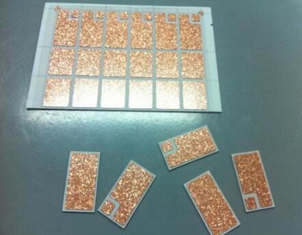
1: The composition of relevant design elements in the PCB should be explained in the design mode. The shape is represented by mechanical levels 1 to 16 (priority) or no-entry level. If used in the PCB design file at the same time, the common shielding layer is used to disable wiring instead of opening holes, and use machine 1 for molding. In the PCB design drawing, a long slot hole or hollow is shown, and the corresponding shape is drawn with the "mechanical 1" layer.
2: Overall dimension tolerance
The PCB size should conform to the design pattern. If no pattern is specified, the dimensional tolerance is .2mm.
3: Flatness (warpage) 0.7%
The concept of stratification?
1: Single-panel draws a signal layer with the top layer, indicating that the line of this layer is a face surface.

2: Draw a line layer (Signal layer) on the bottom layer (bottom layer) of the single panel, indicating that the line of this layer is a surface.
3: The double panel I default to the top layer of the face (that is, the top layer), the silk screen characters sitting on it, the bottom layer (bottom layer) is the face, and the silk screen characters on the bottom layer are opposite;
4: Multi-layer cascading commands provide the protel99se version to the layer stack manager, the protel98 version should provide the logo or software sequence, and the pads series design software for layer commands.
Printed wires and gaskets?
1: PCB layout
The layout, line width and line spacing of printed conductors and pads are determined in principle according to the design pattern. But I will have the following processing method: according to the process requirements, the line width, PAD ring width compensation, our company will generally increase the PAD on the single board to enhance the reliability of customer welding. When the designed row spacing does not meet the process requirements (too dense may affect performance and manufacturability), we will make appropriate adjustments in accordance with the design specifications before production.
In principle, it is recommended that customers design double-layer and multi-layer boards. The inner diameter of the through hole (VIA) is set to be 0.3mm or more, the outer diameter is set to be 0.6mm or more, the component pad is larger than the hole diameter of 50%, and the thickness of the small plate is 6 :
1: Tinplate production line width and line distance are designed to be greater than 6mil. The width of the gold-plating process line is designed to be greater than 4 million to shorten the production cycle and reduce the difficulty of manufacturing.
2: Line width tolerance: The internal control standard of printing line width tolerance is 20%
3: Grid processing In order to avoid blistering and thermal stress on the copper surface after the PCB board is bent during peak printing, it is recommended to make the large copper surface into a grid. The grid spacing is 10 mils (not less than 8 mils), and the grid line width is less than 10 mils (not less than 8 mils).
4: Heat shield (heat insulation pad) processing In large-area grounding (electrical), components that often have feet are connected to it. The processing of the connecting feet should take into account the electrical performance and process requirements, and make a cross flower pad (insulating plate) ), can be made during welding due to excessive cooling of the cross section and the possibility of false welding points is greatly reduced.
5: Inner wire, copper foil isolation drill hole is .3mm. It is recommended to insulate the ground pins of PCB components. The distance between the copper foil and the edge of the board is s.3mm, and the external wiring, the edge of the copper foil board, and the position of the gold finger have no copper foil. Avoid short circuits caused by exposed copper.