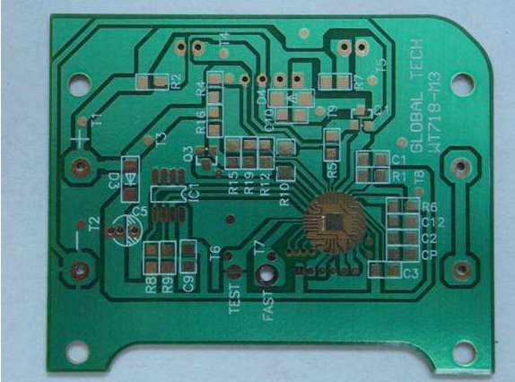
1. In the era of Industry 4.0, how do PCB factories respond?
PCB testing is a key step in PCB manufacturing. It is better to consider it as part of the production itself, rather than as a separate quality control measure. We have written about PCB testing before, especially automatic optical testing and functional testing. The former uses optical methods to determine whether PCB components meet specifications, allowing corrections when any defects occur; the latter test of printed circuit boards is carried out at the end of manufacturing. FCT testing takes longer, but it should also be more thorough to ensure that only functional boards are sent to customers.
However, in this article, we will introduce where PCB testing must start. Since the above-mentioned test method is effective for a single circuit board with a specific purpose, the PCB is required to become less professional in its operation and more connected.
Small devices, connecting devices and equipment that require more heat resistance, vibration, and pollution will require more stringent and extensive PCB testing than the current ones.

If people try to place it in a commercial and industrial environment, the "Internet of Things" may become a misleading concept, not because it will not affect people's perceptions of the future of industry. Specifically, Industry 4.0 has absorbed many core concepts of the Internet of Things-communications, networks, and centralized automated decision-making.
In many manufacturing industries, PCB/SMT has a high degree of automation. However, under the concept of Industry 4.0, it is also facing an increase in labor and various costs, as well as industrial upgrading. What should our processing companies do?
Industry 4.0 should take the integration of industrialization and industrialization as a breakthrough. At present, the SMT/PCB industry has a relatively high degree of automation. You can start with the effective connection of the MES system and the ERP system to improve the informatization capability of the manufacturing industry.
The PCB is expected to include at least some system-on-chip functions, especially wireless communication protocols; it is expected to be developed in remote areas; it is closer to a worse environment. Therefore, PCB testing must adopt new methods to test these new aspects. For example, full compliance with communication standards, range and power consumption are also important determinants of circuit board performance. Reliable and long-running heat and vibration will require more powerful circuits; through traditional printed circuit board testing, qualitative and quantitative elements that cannot be fully evaluated after production.
2. Simple PCB assembly skills and tricks
If you are designing a prototype circuit board, you need to follow some general rules to make the entire PCB manufacturing process go smoothly. Here, we have written some tips and tricks to help beginners assemble their first circuit board like professionals.
Place components
There are three main types of prototype PCBs, single-sided, double-sided, and multilayer. Each type of circuit board has different rules for each component, but based on experience, it is best to place the components on top of the circuit board. It is very important to place all components in specific locations, including switches, connectors, LEDs, mounting holes or heat sinks.
The goal is to minimize the wiring length between components to ensure that the prototype printed circuit board does not short-circuit. By simply putting the components next to each other together, it is easier to lay the path on the road.
The IC should only be placed in one position on the circuit board, up and down or from left to right. Performing more operations may cause confusion on the circuit board. If you leave enough space between these components, you can also save a lot of time, because the trace must be located between them.
After placing all the components correctly, print the layout and place it on the prototype circuit board. In this way, you can check to make sure that each component has enough space without touching each other, and then you can complete the welding process.
Place the ground cable and power cable
After soldering the components, the next step is to lay the power and ground cables. When using an IC, the power line and ground line are critical because they will be connected to the common rail of each power supply. This is a way to avoid daisy chaining power cables from one part to another.
Position signal tracking.
The goal here is to make signal routing as short and direct as possible. Vias (called vias) can move signals from one layer to another, so please use this information. In addition, wiring that carries more current should be wider than any other signal wiring to prevent short circuits.