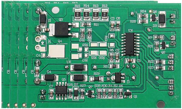
The pre-bake before assembly of the flexible printed circuit board (PCB) is the industry standard requirement of IPC 223 seconds 5.3.5 and IPC-fa-251 seconds. This applies to all flexible and rigid-flex designs based on polyimide. But why pre-bake before assembly, rather than early in the circuit board manufacturing stage?
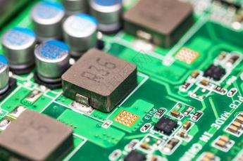
Most flexible circuit designs that require a certain degree of component assembly are made of polyimide materials. Polyimide is used for flexible cores, coatings, and in many cases also reinforcing ribs. The natural inherent characteristic of polyimide is water absorption. At 20°C and 50% relative humidity, it will absorb about 2% of water (by weight). In environments with high humidity and temperature, this may increase. This applies to all polyimide materials from any and all suppliers, and is not an attribute that the flexible PCB manufacturer may influence or modify.
Hygroscopicity of polyimide material

Although the hygroscopicity does not affect the mechanical and electrical properties of the polyimide material, this happens when the components encounter high temperatures during the assembly reflow process.
Specifically, in most cases, the absorbed water is converted to steam during the reflux process. When moisture changes from liquid to gas, it expands, causing delamination between parts. As the temperature required by RoHS increases, this has become a bigger problem. During the assembly process, the only feasible solution to prevent delamination is to pre-bend flexible or rigid bending parts before the assembly process to ensure that the parts are 100% moisture-free. Delamination between FR4 stiffener and flexible circuit. Failure to remove all moisture is the main reason for the delamination of the cover layer, layer by layer and steel layer.
Flexible PCB pre-baking process
PCB baking is usually carried out at 120°C for 2-10 hours. The pre-baking time varies according to the design of specific parts. The number of layers, ribs and structure are factors that increase the required pre-drying time. In addition, the parts need to be placed in the oven so that there is enough airflow around each part.
After the components are pre-baked, it is recommended to take them out of the oven and cool them to working temperature before assembly. Any significant delay will cause the parts to re-absorb moisture. For flexible circuit boards that require multiple assembly cycles, if the time between assembly cycles is extended, a second pre-baking may be required.
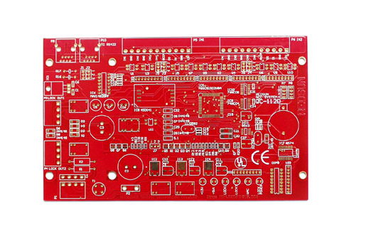
2. Common PCB manufacturing problems: electroplating voids
Plated through holes are copper-plated holes on a printed circuit board (PCB). These holes allow the circuit to pass through the copper in the hole from one side of the circuit board to the other side of the circuit board. For any printed circuit board design with two or more circuit layers, plated through holes form electrical interconnections between the different layers.
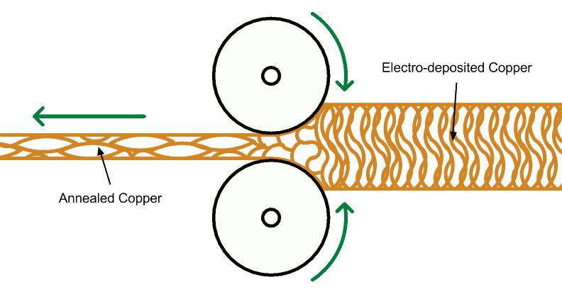
In order to make plated through holes during the PCB manufacturing process, manufacturers drill holes in the circuit board laminate and the foil on both sides. The wall of the hole is then electroplated to transmit the signal from one layer to the other. In order to prepare the circuit board for electroplating, the manufacturer must guide the circuit board from top to bottom through a thin layer of chemically bonded electroless copper that adheres to the inside of the hole and the edge of the circuit board. This step is called copper deposition.
After deposition, the circuit image is applied and developed. Then, the area where the circuit exists is plated with a thicker copper layer, which will cover the hole and the circuit to the final required thickness (usually about .001 inches / .025 mm). From this perspective, the circuit board will continue the manufacturing process until it is completed.
Deposition problem
Deposition problems can affect the interconnection inside the hole wall and cause PCB failure. The most common deposition defect is the plating gap on the copper-lined hole wall. If the hole wall is not smooth and the coating is incomplete, the current cannot pass. The image above shows the cross-section of the through hole, where the copper on the wall is too thin, which may be caused by poor deposition and electroplating.
During the deposition process, when the copper coating is not uniform, plated holes will appear in the plated through holes, which hinders correct plating. This may be caused by contamination, air bubbles on the side of the hole, and/or rough drilling. All of these may form uneven surfaces on the through-hole walls, which makes it difficult to use smooth and continuous copper wires.
Prevent plated holes from appearing on the circuit board
The best way to prevent PCB plating holes from being caused by rough drilling is to ensure that the manufacturer's instructions are followed during use. Manufacturers usually make recommendations for the recommended number of drill bits, drill bit feed rate and speed. Drills with low ROP may actually
Will be crushed.
The resulting material forms a rough surface, which is difficult to coat uniformly during deposition and electroplating. If the ROP is too low, bit contamination may occur, although it can be corrected during the decontamination process.