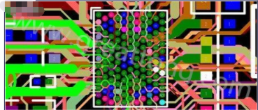
The chip is packaged on the PCB, the semiconductor chip is placed on the printed circuit board, the electrical connection between the chip and the PCB substrate is realized by wire stitching, and the electrical connection between the chip and the substrate is realized by wire stitching, and it is covered with resin to ensure reliability. Although COB is the simplest bare chip mounting technology, its packaging density is far inferior to TAB and flip-chip bonding technology.
The chip on board (COB) process is first to cover the silicon wafer placement point with a thermally conductive epoxy resin (generally silver-doped epoxy resin) on the surface of the substrate, and then place the silicon wafer directly on the surface of the substrate and heat treatment Until the silicon chip is firmly fixed on the substrate, then wire bonding is used to directly establish an electrical connection between the silicon chip and the substrate.
Compared with other packaging technologies, COB technology is inexpensive, space-saving, and mature. However, any* technology was impossible to be perfect when it first appeared. COB technology also has disadvantages such as the need for additional welding machines and packaging machines, sometimes the speed cannot keep up, and the stricter environmental requirements of the PCB patch and the inability to maintain it.
Certain chip-on-board (CoB) layouts can improve IC signal performance because they remove most or all of the package, that is, remove most or all of the parasitic components. However, with these technologies, there may be some performance issues. In all these designs, the substrate may not be well connected to VCC or ground due to the lead frame chip or BGA logo. Possible problems include coefficient of thermal expansion (CTE) issues and poor substrate connections.
The main welding methods of COB:

(1) Hot pressure welding
The metal wire and the welding zone are pressure-welded together by heating and pressure. The principle is to plastically deform the welding area (such as AI) and destroy the oxide layer on the pressure welding interface through heating and pressure, so that the attraction between atoms is achieved to achieve the purpose of "bonding". In addition, the two metal interfaces are not When leveling, heating and pressurizing, the upper and lower metals can be inlaid with each other. This technology is generally used as chip-on-glass COG.
(2) Ultrasonic welding
Ultrasonic welding uses the energy generated by an ultrasonic generator. The transducer rapidly expands and contracts under the induction of an ultra-high frequency magnetic field to produce elastic vibration, which makes the wedge vibrate correspondingly, and at the same time exerts a certain pressure on the wedge, so the wedge is in Under the combined action of these two forces, the AI wire is quickly rubbed on the surface of the metalized layer (AI film) in the welded area, causing plastic deformation of the surface of the AI wire and the AI film. This deformation also destroys the interface of the AI layer. The oxide layer brings the two pure metal surfaces into close contact to achieve the bond between atoms, thus forming a weld. The main welding material is aluminum wire welding head, generally wedge-shaped.
(3) Gold wire welding
Ball bonding is the most representative bonding technology in wire bonding, because the current semiconductor package secondary and triode packages all use AU wire ball bonding. Moreover, it is easy to operate, flexible, strong in welding points (the welding strength of AU wire with a diameter of 25UM is generally 0.07~0.09N/point), and it has no directionality, and the welding speed can be as high as 15 points/sec. Gold wire bonding is also called hot (pressure) (ultra) acoustic welding. The main bonding material is gold (AU) wire. The head is spherical, so it is ball bonding.
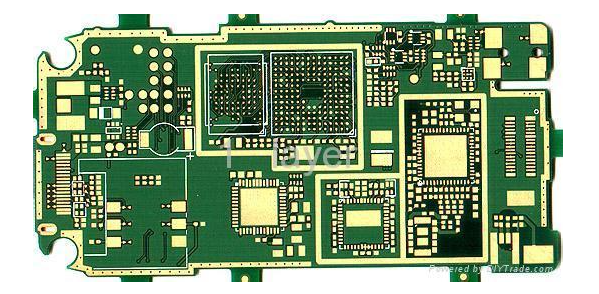
COB packaging process
The first step: crystal expansion. The expansion machine is used to expand the entire LED chip film provided by the manufacturer evenly, so that the tightly arranged LED dies attached to the surface of the film are pulled apart, which is convenient for thorns.
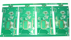
Step 2: Adhesive. Place the expanded crystal ring on the backing machine surface where the silver paste layer has been scraped, and put the silver paste on the back. Some silver paste. Suitable for bulk LED chips. Use a dispensing machine to spot an appropriate amount of silver paste on the PCB printed circuit board.
The third step: Put the crystal expansion ring prepared with silver paste into the piercing crystal holder, and the operator will pierce the LED chip on the PCB printed circuit board with a piercing pen under the microscope.
Step 4: Put the pierced PCB printed circuit board in a thermal cycle oven and let it stand for a period of time. After the silver paste is cured, take it out (not for a long time, otherwise the coating of the LED chip will be yellowed, that is, oxidized. Cause difficulties). If there is LED chip bonding, the above steps are required; if there is only IC chip bonding, the above steps are canceled.
The fifth step: stick the chip. Use a dispenser to put an appropriate amount of red glue (or black glue) on the IC position on the PCB printed circuit board, and then use an anti-static device (vacuum suction pen or sub) to correctly place the IC die on the red glue or black glue.
The sixth step: drying. Put the glued die in a thermal cycle oven on a large flat heating plate and let it stand at a constant temperature for a period of time, or it can be cured naturally (for a longer time).
Step 7: Bonding (wire bonding). The aluminum wire bonding machine is used to bridge the chip (LED die or IC chip) with the aluminum wire of the corresponding pad on the PCB board, that is, the inner lead of the COB is welded.
The eighth step: pre-test. Use special testing tools (different equipment for COB for different purposes, simply high-precision regulated power supply) to test the COB board, and re-repair the unqualified board.
Step 9: Dispensing. A glue dispenser is used to place an appropriate amount of the prepared AB glue onto the bonded LED die, and the IC is packaged with black glue, and then packaged in appearance according to customer requirements.
The tenth step: curing. Put the sealed PCB printed circuit board into a thermal cycle oven and let it stand at a constant temperature. Different drying times can be set according to requirements.
The eleventh step: post-test. The packaged PCB printed circuit boards are then tested for electrical performance with special testing tools to distinguish between good and bad.