Wafer level packaging (WLCSP) is a CSP packaging technology that enables integrated circuits (ICs) to be mounted face down on printed circuit boards. The solder joints of the chip are soldered to the PCB pads through separate solder balls. Any filling material. This technology differs from ball grid array, lead type, and laminate-based CSP packaging technology in that it has no wires or plug-in connections. The first advantage of WLCSP packaging technology is that the inductance between the IC and the PCB is very small. The second advantage is to reduce the package size and production cycle, and improve the thermal conductivity. Maxim's WLCSP technology trademark is UCSP.
The UCSP package structure surface provides electrical isolation. A photographic method is used to make vias on the BCB film, through which the electrical connection with the IC connection substrate can be realized. A UBM (Under Ball Metal) layer is also added to the via. In general, a second layer of BCB is added as a solder mask to determine the diameter and position of the reflow solder ball. The standard tin ball material is eutectic tin-lead alloy, which is 63%Sn/37%Pb. A cross-sectional view of a typical UCSP structure.

A cross-sectional view of a typical UCSP structure. The UCSP solder ball array is based on a rectangular grid arrangement with a uniform grid pitch. The number of rows and columns of the UCSP solder ball array is generally between 2 and 6.
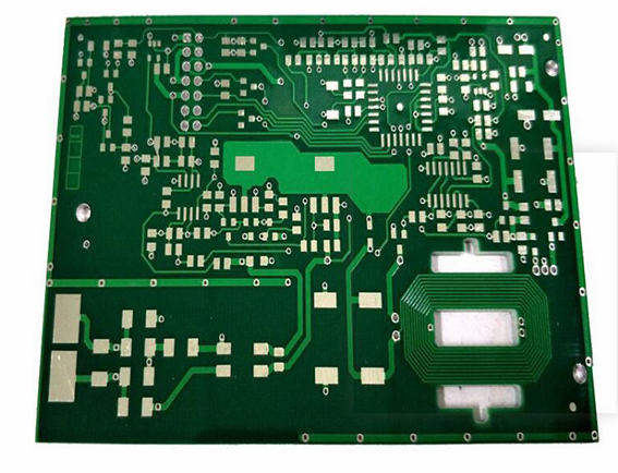
The design principles of UCSP pad structure and PCB manufacturing specifications To successfully use UCSP components in assembly, it is necessary to pay attention to the problem of circuit board layout. The layout and manufacturing of the printed circuit board (PCB) will affect the UCSP assembly yield, equipment performance and solder joint reliability. The design principles and PCB manufacturing specifications of the UCSP pad structure are different from lead-type devices and laminate-based BGA devices.
Solder mask defined (SMD) and non-solder mask defined (NSMD) from the previous content, we can see that the pad structure for surface mount components has solder mask defined (Solder-Mask Defined, SMD) and non-solder mask defined (Non-Solder-Mask Defined, NSMD) two forms. When designing the PCB, the requirements of power, grounding and signal direction must be considered, and one should be selected between NSMD and SMD pads. The special micro-via design may avoid surface wiring, but it requires more advanced board manufacturing technology. Once selected, UCSP pad types cannot be mixed. The layout of the UCSP pad and the wires connected to it should be symmetrical to prevent off-center wetting.
1: The process of etching copper wires can be better controlled. Compared with the solder mask etching when using SMD pads, NSMD is a better choice.
2: SMD pads may cause concentrated pressure where the solder mask overlaps, which will cause the solder joints to crack when the pressure is too high.
3: According to the production rules of copper wires and other open ground on the PCB, NSMD pads can provide more space for PCB wiring.
4: Compared with SMD pads, the larger solder mask opening of NSMD provides a larger working window for the placement of UCSP components.
5: SMD pads can use wider copper wires and have lower inductance in connection with power and ground.
6: PCB company used NSMD design in temperature cycling test.