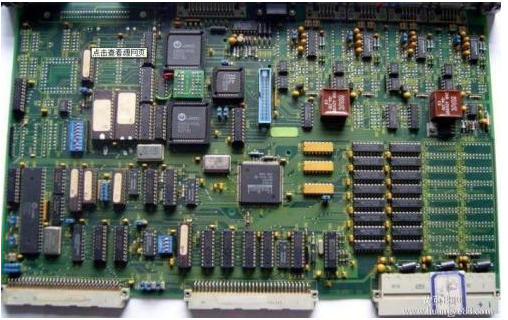
The basic principles of PCB proofing circuit board layout are as follows:
1: Taking into account the distribution parameters of circuit components under high-frequency working conditions, all components should be uniformly, neatly, and compactly arranged on the double-sided circuit board to minimize and shorten the lead length between the components.
2: The analog circuit should be separated from the digital circuit. The interference of digital signals to analog signals is eliminated.
3: Arrange the location of the clock circuit reasonably.
The clock circuit cannot be directly connected to the signal line, it is located in the center of the double-sided circuit board and grounded. The layout of the optical burst module circuit can be considered from the following four aspects:
1: The position of the laser MAX3656 and the plug-in is preset by the SFMSA specification, and the laser and the driver are as close as possible.

2: The position of the limiting amplifier MAX3747 is as close as possible to the back-end main amplifier chip MAX3748 to ensure the correct reception of the signal direction and the amplified signal, and to minimize interference.
3: The clock and data recovery circuit MAX3872 should be placed at the center and reliable ground.
4: Consider using the MAX3654-47-870MHz analog CATV inter-block amplifier as a functional module area for combined processing.
First, expand the package library to meet the needs of layout and wiring design, and then the relevant software directly calls the component package symbols to complete the preliminary layout and wiring design of the circuit. After preliminarily determining the layout of most components, simulation analysis is usually performed before and after wiring. The main simulation analysis before PCB wiring.
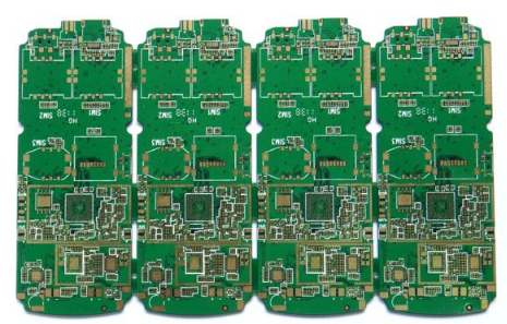
2. How to control PCB cost
In PCB design, the main factors affecting cost are the following four points.
1: PCB layers:
Generally, the more PCB layers with the same area, the higher the price. The design engineer should use a small number of layers to complete the PCB design while ensuring the quality of the design signal.
2: PCB size
With a certain number of layers, the smaller the size of the PCB, the lower the price. The design engineer will not affect the electrical performance when designing the PCB. If the size of the PCB can be reduced, the size and cost can be reduced reasonably.
3: Easy to make
The main parameters that affect PCB manufacturing are minimum line width, minimum line spacing, minimum punching, etc. If these parameters are set too small or the process capability has reached the minimum limit of the PCB factory, the yield of PCB will be reduced and the production cost will increase. . Therefore, when designing the PCB process, it is necessary to avoid challenging the limits of the factory, setting reasonable line width and line spacing, and punching. Similarly, through holes can be designed, try not to use HDI blind holes, because the processing process of blind holes is much more difficult than through holes, which will increase the production cost of PCB.
4: PCB board material
There are many classifications of PCB boards, common paper-based printed circuit boards, epoxy glass fiber cloth printed circuit rice composite substrate printed circuit boards, special substrate printed circuit board metal substrates. The processing gap of different materials is very large, and the processing cycle of some special materials will be longer. Therefore, when designing, it is necessary to select as much as possible the more common and affordable materials that meet the design requirements, such as RF4 materials.